- 您現(xiàn)在的位置:買賣IC網(wǎng) > PDF目錄384208 > CL7128SQC100-6 PDF資料下載
參數(shù)資料
| 型號: | CL7128SQC100-6 |
| 文件頁數(shù): | 11/14頁 |
| 文件大?。?/td> | 107K |
| 代理商: | CL7128SQC100-6 |
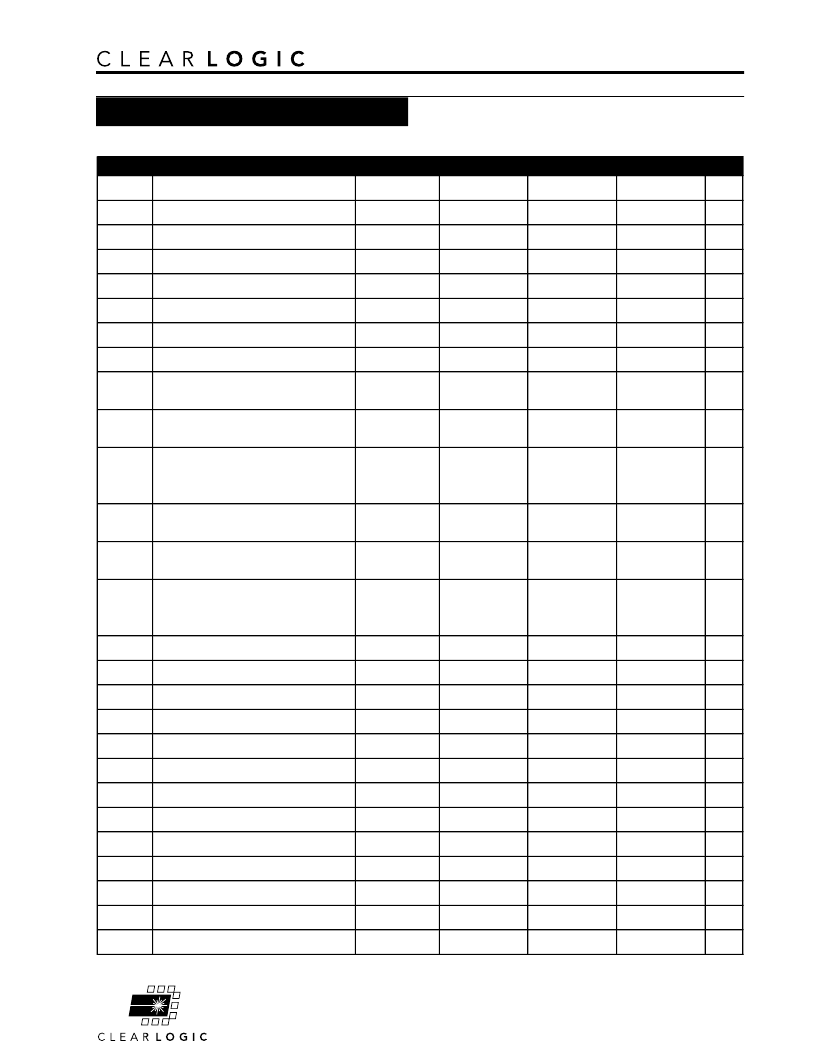
CL7128A and CL7128AE Laser Processed Logic Devices
Page 73
Parameter
Conditions
Min
Max
Min
Max
Min
Max
Unit
t
iN
Input pad and buffer delay
0.4
0.6
0.7
ns
t
IO
I/O input pad and buffer delay
0.4
0.6
0.7
ns
t
FIN
Fast input delay
3.3
3.7
4.1
ns
t
SEXP
Shared expander delay
3.6
4.9
5.9
ns
t
PEXP
Parallel expander delay
0.8
1.1
1.3
ns
t
LAD
Logic array delay
3.7
5.0
6.0
ns
t
LAC
Logic control array delay
3.4
4.6
5.6
ns
t
IOE
Internal output enable delay
0.0
0.0
0.0
ns
Output buffer and pad delay
Slow slew rate = off, V
CCIO
= 5.0 V
Output buffer and pad delay
Slow slew rate = off, V
CCIO
= 3.3 V
Output buffer and pad delay
Slow slew rate = on,
V
CCIO
= 5.0 V or 3.3 V
Output buffer enable delay
Slow slew rate = off, V
CCIO
= 5.0 V
Output buffer enable delay
Slow slew rate = off, V
CCIO
= 3.3 V
Output buffer enable delay
Slow slew rate = on,
V
CCIO
= 5.0 V or 3.3 V
t
XZ
Output buffer disable delay
C
L
= 5 pF
[3]
4.0
5.0
5.0
ns
t
SU
Register setup time
1.3
1.7
2.0
ns
t
H
Register hold time
2.4
3.8
4.8
ns
t
FSU
Register setup time of fast input
1.1
1.1
1.1
ns
t
FH
Register hold time of fast input
1.9
1.9
1.9
ns
t
RD
Register delay
2.1
2.8
3.3
ns
t
COMB
Combinatorial delay
1.5
2.0
2.4
ns
t
IC
Array clock delay
3.4
4.6
5.6
ns
t
EN
Register enable time
3.4
4.6
5.6
ns
t
GLOB
Global control delay
1.4
1.8
2.2
ns
t
PRE
Register preset time
3.9
5.2
6.2
ns
t
CLR
Register clear time
3.9
5.2
6.2
ns
t
LIA
LIA delay
1.3
1.7
2.0
ns
Speed: -7
Speed: -10
Speed: -12
Symbol
t
OD1
C
L
= 35 pF
0.6
0.7
0.9
ns
t
OD2
C
L
= 35 pF
1.1
1.2
0.4
ns
t
OD3
C
= 35 pF
5.6
5.7
5.9
ns
t
ZX1
C
L
= 35 pF
4.0
5.0
5.0
ns
t
ZX2
C
L
= 35 pF
4.5
5.5
9.0
10.0
t
ZX3
C
L
= 35 pF
10.0
ns
7KA tbl 07A2
5.5
ns
AC Electrical Specifications cont.
Internal T iming Parameters
[4]
相關(guān)PDF資料 |
PDF描述 |
|---|---|
| CL7128SQC100-7 | Laser-Programmable Complex PLD |
| CL7128SQC160-10 | |
| CL7128SQC160-15 | Laser-Programmable Complex PLD |
| CL7128STI100-10 | |
| CL7160ELC84-10 | Laser-Programmable Complex PLD |
相關(guān)代理商/技術(shù)參數(shù) |
參數(shù)描述 |
|---|---|
| CL7163-000 | 制造商:TE Connectivity 功能描述:44A9748-20-9-9CS3185 - Cable Rools/Shrink Tubing |
| CL7174-000 | 制造商:TE Connectivity 功能描述:Heat Shrink Tubing 制造商:TE Connectivity 功能描述:202K121-25-01/225-0-CS8387 - Bulk |
| CL72001X | 制造商:BANDRIDGE 功能描述:LEAD AV CAT5 0.5M |
| CL72002X | 制造商:BANDRIDGE 功能描述:LEAD AV CAT5 2M |
| CL72003X | 制造商:BANDRIDGE 功能描述:LEAD AV CAT5 3M |
發(fā)布緊急采購,3分鐘左右您將得到回復(fù)。