- 您現(xiàn)在的位置:買賣IC網(wǎng) > PDF目錄379856 > CDP1824EX (INTERSIL CORP) 32-Word x 8-Bit Static RAM PDF資料下載
參數(shù)資料
| 型號: | CDP1824EX |
| 廠商: | INTERSIL CORP |
| 元件分類: | DRAM |
| 英文描述: | 32-Word x 8-Bit Static RAM |
| 中文描述: | 32 X 8 STANDARD SRAM, 710 ns, PDIP18 |
| 封裝: | PLASTIC, DIP-18 |
| 文件頁數(shù): | 4/5頁 |
| 文件大?。?/td> | 111K |
| 代理商: | CDP1824EX |
45
All Intersil U.S. products are manufactured, assembled and tested utilizing ISO9000 quality systems.
Intersil Corporation’s quality certifications can be viewed at www.intersil.com/design/quality
Intersil products are sold by description only. Intersil Corporation reserves the right to make changes in circuit design, software and/or specifications at any time without
notice. Accordingly, the reader is cautioned to verify that data sheets are current before placing orders. Information furnished by Intersil is believed to be accurate and
reliable. However, no responsibility is assumed by Intersil or its subsidiaries for its use; nor for any infringements of patents or other rights of third parties which may result
from its use. No license is granted by implication or otherwise under any patent or patent rights of Intersil or its subsidiaries.
For information regarding Intersil Corporation and its products, see www.intersil.com
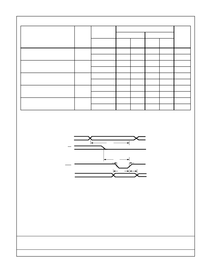
Write Cycle Dynamic Electrical Specifications
Input t
R
, t
F
≤
15ns, C
L
= 50pF
PARAMETER
SYMBOL
TEST
CONDITIONS
LIMITS
UNITS
-55
o
C, +25
o
C
+125
o
C
V
DD
(V)
(NOTE 1)
MIN
MAX
(NOTE 1)
MIN
MAX
Write Pulse Width
t
WRW
5
350
-
475
-
ns
10
180
-
220
-
ns
Data Setup Time
t
DS
5
400
-
560
-
ns
10
190
-
260
-
ns
Data Hold Time
t
DH
5
70
-
90
-
ns
10
35
-
45
-
ns
Chip Select Setup Time
t
CS
5
550
-
775
-
ns
10
340
-
475
-
ns
Address Setup Time
t
AS
5
550
-
775
-
ns
10
340
-
475
-
ns
NOTE:
1. Time required by a device to allow for the indicated function.
FIGURE 2. WRITE CYCLE TIMING DIAGRAM
MA
CS
MWR
BUS
t
AS
t
CS
t
WRW
t
DS
t
DH
CDP1824/3, CDP1824C/3
相關(guān)PDF資料 |
PDF描述 |
|---|---|
| CDP1824 | 32-Word x 8-Bit Static RAM |
| CDP1824C | 32-Word x 8-Bit Static RAM |
| CDP1824D | 32-Word x 8-Bit Static RAM |
| CDP1824E | 32-Word x 8-Bit Static RAM |
| CDP1824CD | 32-Word x 8-Bit Static RAM |
相關(guān)代理商/技術(shù)參數(shù) |
參數(shù)描述 |
|---|---|
| CDP1826C | 制造商:INTERSIL 制造商全稱:Intersil Corporation 功能描述:CMOS 64-Word x 8-Bit Static RAM |
| CDP1826CD | 制造商:Harris Corporation 功能描述: |
| CDP1826CE | 制造商:INTERSIL 制造商全稱:Intersil Corporation 功能描述:CMOS 64-Word x 8-Bit Static RAM |
| CDP1826CE WAF | 制造商:Harris Corporation 功能描述: |
| CDP1832 WAF | 制造商:Harris Corporation 功能描述: |
發(fā)布緊急采購,3分鐘左右您將得到回復(fù)。