- 您現(xiàn)在的位置:買賣IC網(wǎng) > PDF目錄375676 > CDALA10M7GA086 (Murata Manufacturing Co., Ltd.) Ceramic Filters (CERAFIL) for FM Receivers PDF資料下載
參數(shù)資料
| 型號: | CDALA10M7GA086 |
| 廠商: | Murata Manufacturing Co., Ltd. |
| 英文描述: | Ceramic Filters (CERAFIL) for FM Receivers |
| 中文描述: | 陶瓷濾波器(濾波器陶瓷濾波器)的調(diào)頻接收器 |
| 文件頁數(shù): | 7/57頁 |
| 文件大小: | 992K |
| 代理商: | CDALA10M7GA086 |
第1頁第2頁第3頁第4頁第5頁第6頁當(dāng)前第7頁第8頁第9頁第10頁第11頁第12頁第13頁第14頁第15頁第16頁第17頁第18頁第19頁第20頁第21頁第22頁第23頁第24頁第25頁第26頁第27頁第28頁第29頁第30頁第31頁第32頁第33頁第34頁第35頁第36頁第37頁第38頁第39頁第40頁第41頁第42頁第43頁第44頁第45頁第46頁第47頁第48頁第49頁第50頁第51頁第52頁第53頁第54頁第55頁第56頁第57頁
Please read CAUTION and Notice in this catalog for safety. This catalog has only typical specifications. Therefore you are requested
to approve our product specification or to transact the approval sheet for product specification, before your ordering.
P61E7.pdf 01.10.17
Chip CERAFIL
r
SFECV Series Notice
6
1
I
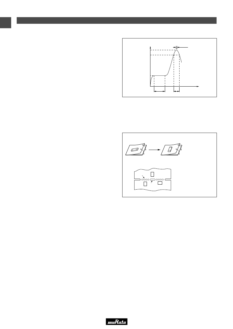
Notice (Soldering and Mounting)
1. Standard Reflow Soldering Condition
(1) Reflow
The component cannot be withstand washing.
2. Wash
Lead terminal is directly contacted with the tip of
soldering iron of 280
±
5C for 3.0
±
0.5 seconds.
(2) Soldering Iron
60
30
Time(sec.)
5sec.
150
230
240
T
°
C
Gradual Cooling
I
Notice (Handling)
1. The component will be damaged when an excessive
stress is applied.
2. The component may be damaged if excess mechanical
stress is applied to it mounted on the printed circuit
board.
3. Design layout of components on the PC board to
minimize the stress imposed on the warp or flexure of the
board.
4. After installing chips, if solder is excessively applied to
the circuit board, mechanical stress will cause
destruction resistance characteristics to lower. To
prevent this, be extremely careful in determining shape
and dimension before designing the circuit board
diagram.
5. When the positioning claws and pick up nozzle are worn,
the load is applied to the chip while positioning is
concentrated to one positioning accuracy, etc. Careful
checking and maintenance are necessary to prevent
unexpected trouble.
6. When correcting chips with a soldering iron, the tip of the
soldering iron should not directly touch the chip
component. Depending on the soldering conditions, the
effective area of terminations may be reduced. the use of
solder containing Ag should be done to prevent the
electrode erosion.
7. Do not clean or wash the component as it is not
hermetically sealed.
8. In case of covering filter with over coat, conditions such
as material of resin, cure temperature, and so on should
be evaluated well.
9. Do not use strong acidity flux, more than 0.2wt% chlorine
content, in re-flow soldering.
10. Accurate test circuit values are required to measure
electrical characteristics.It may be a cause of mis-
correlation if there is any deviation, especially stray
capacitance, from the test circuit in the specification.
[Component direction]
[Component layout close to board]
Put the
component
lateral to the
direction in
which stress
acts.
Susceptibility to
stress is in the order
of : A>C>B
B
A
C
Slit
Perforation
相關(guān)PDF資料 |
PDF描述 |
|---|---|
| CDALA10M7GA087 | Ceramic Filters (CERAFIL) for FM Receivers |
| CDALA10M7GA088 | Ceramic Filters (CERAFIL) for FM Receivers |
| CDALA10M7GA089 | Ceramic Filters (CERAFIL) for FM Receivers |
| CDALA10M7GA090 | Ceramic Filters (CERAFIL) for FM Receivers |
| CDALA10M7GA091 | Ceramic Filters (CERAFIL) for FM Receivers |
相關(guān)代理商/技術(shù)參數(shù) |
參數(shù)描述 |
|---|---|
| CDALA10M7GA087 | 制造商:MURATA 制造商全稱:Murata Manufacturing Co., Ltd. 功能描述:Ceramic Filters (CERAFIL) for FM Receivers |
| CDALA10M7GA088 | 制造商:MURATA 制造商全稱:Murata Manufacturing Co., Ltd. 功能描述:Ceramic Filters (CERAFIL) for FM Receivers |
| CDALA10M7GA089 | 制造商:MURATA 制造商全稱:Murata Manufacturing Co., Ltd. 功能描述:Ceramic Filters (CERAFIL) for FM Receivers |
| CDALA10M7GA090 | 制造商:MURATA 制造商全稱:Murata Manufacturing Co., Ltd. 功能描述:Ceramic Filters (CERAFIL) for FM Receivers |
| CDALA10M7GA091 | 制造商:MURATA 制造商全稱:Murata Manufacturing Co., Ltd. 功能描述:Ceramic Filters (CERAFIL) for FM Receivers |
發(fā)布緊急采購,3分鐘左右您將得到回復(fù)。