- 您現(xiàn)在的位置:買賣IC網(wǎng) > PDF目錄366832 > CD4024AD Logic IC PDF資料下載
參數(shù)資料
| 型號(hào): | CD4024AD |
| 英文描述: | Logic IC |
| 中文描述: | 邏輯IC |
| 文件頁(yè)數(shù): | 4/9頁(yè) |
| 文件大?。?/td> | 99K |
| 代理商: | CD4024AD |
www.fairchildsemi.com
4
C
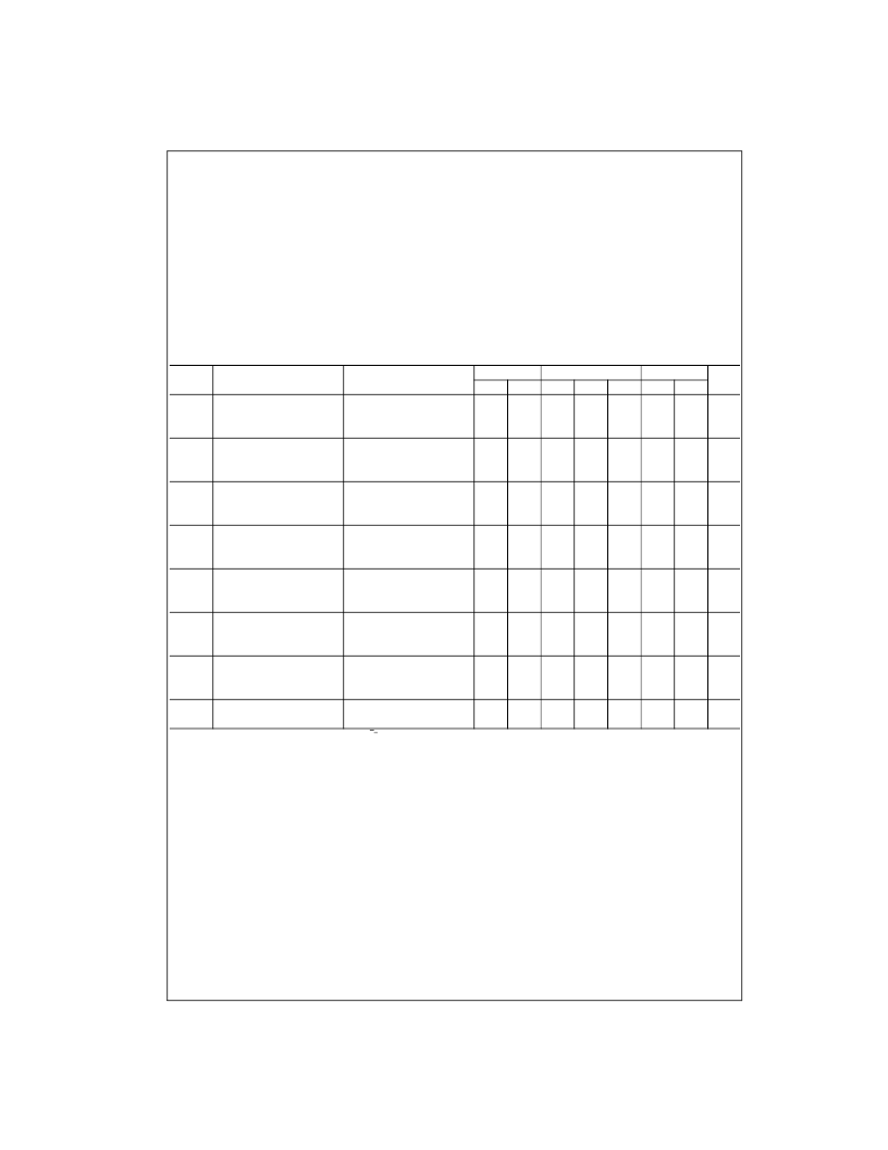
Absolute Maximum Ratings
(Note 1)
(Note 2)
Recommended Operating
Conditions
Note 1:
“
Absolute Maximum Ratings
”
are those values beyond which the
safety of the device cannot be guaranteed. They are not meant to imply
that the devices should be operated at these limits. The tables of
“
Recom-
mended Operating Conditions
”
and
“
Electrical Characteristics
”
provide con-
ditions for actual device operation.
Note 2:
V
SS
=
0V unless otherwise specified.
DC Electrical Characteristics
(Note 2)
Note 3:
Data does not apply to oscillator points
φ
0
and
φ
0
of CD4060BC. I
OH
and I
OL
are tested one output at a time.
Supply Voltage (V
DD
)
Input Voltage (V
IN
)
Storage Temperature Range (T
S
)
Package Dissipation (P
D
)
Dual-In-Line
Small Outline
Lead Temperature (T
L
)
(Soldering, 10 seconds)
0.5V to
+
18V
0.5V to V
DD
+
0.5V
65
°
C to
+
150
°
C
700 mW
500 mW
260
°
C
Supply Voltage (V
DD
)
Input Voltage (V
IN
)
Operating Temperature Range (T
A
)
+
3V to
+
15V
0V to V
DD
55
°
C to
+
125
°
C
Symbol
Parameter
Conditions
55
°
C
Min
+
25
°
C
Typ
+
125
°
C
Min
Units
Max
5
10
Min
Max
5
10
Max
150
300
I
DD
Quiescent Device Current
V
DD
=
5V, V
IN
=
V
DD
or V
SS
V
DD
=
10V, V
IN
=
V
DD
or V
SS
V
DD
=
15V, V
IN
=
V
DD
or V
SS
V
DD
=
5V
V
DD
=
10V
V
DD
=
15V
V
DD
=
5V
V
DD
=
10V
V
DD
=
15V
V
DD
=
5V, V
O
=
0.5V or 4.5V
V
DD
=
10V, V
O
=
1.0V or 9.0V
V
DD
=
15V, V
O
=
1.5V or 13.5V
V
DD
=
5V, V
O
=
0.5V or 4.5V
V
DD
=
10V, V
O
=
1.0V or 9.0V
V
DD
=
15V, V
O
=
1.5V or 13.5V
V
DD
=
5V, V
O
=
0.4V
V
DD
=
10V, V
O
=
0.5V
V
DD
=
15V, V
O
=
1.5V
V
DD
=
5V, V
O
=
4.6V
V
DD
=
10V, V
O
=
9.5V
V
DD
=
15V, V
O
=
13.5V
V
DD
=
15V, V
IN
=
0V
V
DD
=
15V, V
IN
=
15V
μ
A
20
0.05
0.05
20
0.05
0.05
600
0.05
0.05
V
OL
LOW Level Output Voltage
0
0
V
0.05
0
5
0.05
0.05
V
OH
HIGH Level Output Voltage
4.95
9.95
4.95
9.95
4.95
9.95
V
10
14.95
14.95
15
2
4
14.95
V
IL
LOW Level Input Voltage
1.5
3.0
1.5
3.0
1.5
3.0
V
4.0
6
3
6
4.0
4.0
V
IH
HIGH Level Input Voltage
3.5
7.0
3.5
7.0
3.5
7.0
V
11.0
0.64
1.6
11.0
0.51
1.3
9
11.0
0.36
0.9
I
OL
LOW Level Output Current
(Note 3)
0.88
2.25
mA
4.2
0.64
1.6
4.2
3.4
0.51
1.3
3.4
8.8
0.88
2.25
8.8
10
5
10
5
2.4
0.36
0.9
2.4
I
OH
HIGH Level Output Current
(Note 3)
mA
I
IN
Input Current
0.1
0.1
0.1
0.1
1.0
1.0
μ
A
相關(guān)PDF資料 |
PDF描述 |
|---|---|
| CD4024AE | Logic IC |
| CD4025CJ | Triple 3-input NAND Gate |
| CD4025CN | Triple 3-input NAND Gate |
| CD4025MD | Triple 3-input NAND Gate |
| CD4025MF | Triple 3-input NAND Gate |
相關(guān)代理商/技術(shù)參數(shù) |
參數(shù)描述 |
|---|---|
| CD4024AD3 | 制造商:Rochester Electronics LLC 功能描述:- Bulk |
| CD4024AF | 制造商:RCA 功能描述:Counter, Up, 7 Bit Binary, 14 Pin, Ceramic, DIP |
| CD4024AK3 | 制造商:Rochester Electronics LLC 功能描述:- Bulk |
| CD4024AT | 制造商:Rochester Electronics LLC 功能描述:- Bulk |
| CD4024BCM | 功能描述:計(jì)數(shù)器 IC 7-Stage Binary Ctr RoHS:否 制造商:NXP Semiconductors 計(jì)數(shù)器類型:Binary Counters 邏輯系列:74LV 位數(shù):10 計(jì)數(shù)法: 計(jì)數(shù)順序: 工作電源電壓:1 V to 5.5 V 工作溫度范圍:- 40 C to + 125 C 封裝 / 箱體:SOT-109 封裝:Reel |
發(fā)布緊急采購(gòu),3分鐘左右您將得到回復(fù)。