- 您現(xiàn)在的位置:買賣IC網(wǎng) > PDF目錄374141 > CBT3125 (Texas Instruments, Inc.) QUADRUPLE FET BUS SWITCH PDF資料下載
參數(shù)資料
| 型號: | CBT3125 |
| 廠商: | Texas Instruments, Inc. |
| 英文描述: | QUADRUPLE FET BUS SWITCH |
| 中文描述: | 四路場效應(yīng)管總線開關(guān) |
| 文件頁數(shù): | 4/10頁 |
| 文件大小: | 96K |
| 代理商: | CBT3125 |
Philips Semiconductors
Product data
CBT3125
Quadruple FET bus switch
2001 Dec 12
4
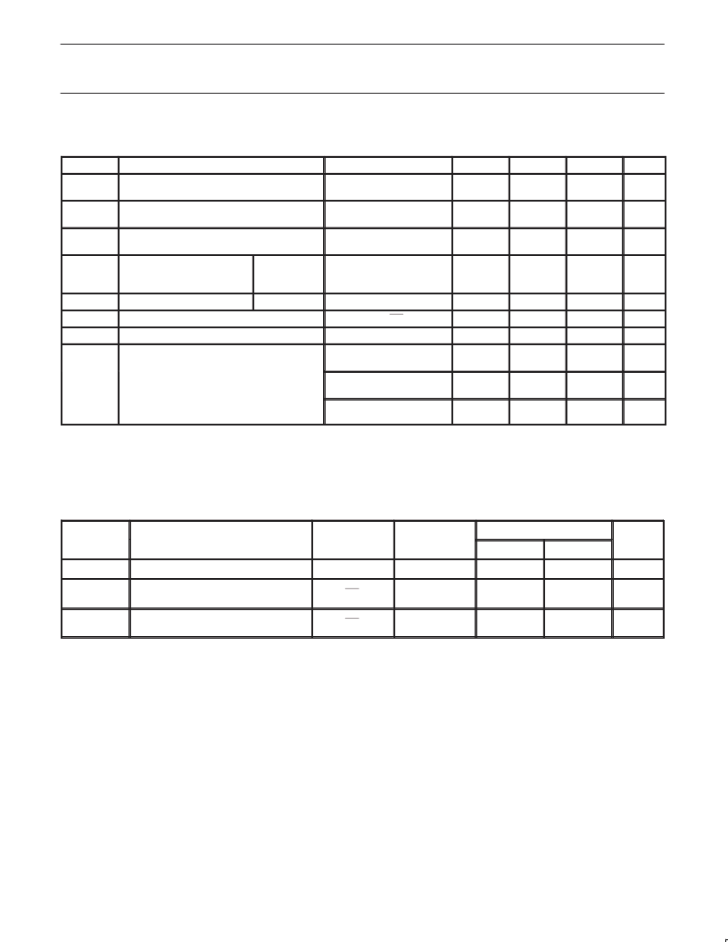
DC ELECTRICAL CHARACTERISTICS
Over recommended operating free-air temperature range, unless otherwise noted.
SYMBOL
PARAMETER
CONDITIONS
MIN.
TYP.
1
MAX.
UNIT
V
IK
Input clamp voltage
V
CC
= 4.5 V;
I
I
= –18 mA
V
CC
= 5.5 V;
V
I
= 5.5 V or GND
V
CC
= 5.5 V; I
O
= 0;
V
I
= V
CC
or GND
V
CC
= 5.5 V;
one input at 3.4 V,
other inputs at V
CC
or GND
V
I
= 3 V or 0
V
O
= 3 V or 0; OE = V
CC
V
CC
= 5.0 V; V
I
= 5.0 V
V
CC
= 4.5 V; V
I
= 0 V;
I
I
= 64 mA
V
= 4.5 V; V
I
= 0 V;
I
I
= 30 mA
V
= 4.5 V; V
I
= 2.4 V;
I
I
= –15 mA
—
—
–1.2
V
I
I
Input leakage current
—
—
±
1
μ
A
I
CC
Quiescent supply current
—
—
3
μ
A
I
CC
Additional supply current per
input pin (Note 2)
control inputs
—
—
2.5
mA
C
I
Input capacitance
control inputs
—
1.7
—
pF
C
IO(OFF)
V
P
Power-off leakage current
—
3.4
—
pF
Pass gate voltage
—
3.8
—
V
—
5
7
r
on
On-resistance (Note 3)
—
5
7
—
10
15
NOTES:
1. All typical values are at V
CC
= 5 V, unless otherwise noted. T
amb
= 25
°
C.
2. This is the increase in supply current for each input that is at the specified TTL voltage level rather than V
CC
or GND.
3. Measured by the voltage drop between the A and the B terminals at the indicated current through the switch. On-state resistance is
determined by the lower of the voltages of the two (A or B) terminals.
AC CHARACTERISTICS
T
amb
= –40 to +85
°
C; C
L
= 50 pF, unless otherwise noted.
SYMBOL
PARAMETER
FROM
(INPUT)
TO
V
CC
= 5 V
±
0.5 V
UNIT
(OUTPUT)
Min
Max
t
pd
Propagation delay
1
A or B
B or A
—
0.25
ns
t
en
Output enable time
to High and Low level
OE
A or B
1.0
5.4
ns
t
dis
Output disable time
from High and Low level
OE
A or B
1
4.7
ns
NOTE:
1. This parameter is warranted but not production tested. The propagation delay is based on the RC time constant of the typical on-state
resistance of the switch and a load capacitance of 50 pF, when driven by an ideal voltage source (zero output impedance).
相關(guān)PDF資料 |
PDF描述 |
|---|---|
| CBT3251 | CBT3251 1-of-8 FET multiplexer/demultiplexer |
| CBT3257 | LC2MOS ±15 V Quad SPST Switch; Package: PLCC; No of Pins: 20; Temperature Range: Commercial |
| CBT3257D | Quad 1-of-2 multiplexer/demultiplexer |
| CBT3257DB | LC2MOS ±15 V Quad SPST Switch; Package: SOIC; No of Pins: 16; Temperature Range: Commercial |
| CBT3257DS | Quad 1-of-2 multiplexer/demultiplexer |
相關(guān)代理商/技術(shù)參數(shù) |
參數(shù)描述 |
|---|---|
| CBT3125D | 功能描述:數(shù)字總線開關(guān) IC QUAD FET BUS SWITCH RoHS:否 制造商:Texas Instruments 開關(guān)數(shù)量:24 傳播延遲時間:0.25 ns 最大工作溫度:+ 85 C 最小工作溫度:- 40 C 封裝 / 箱體:TSSOP-56 封裝:Reel |
| CBT3125D,112 | 功能描述:數(shù)字總線開關(guān) IC QUAD FET BUS SWITCH RoHS:否 制造商:Texas Instruments 開關(guān)數(shù)量:24 傳播延遲時間:0.25 ns 最大工作溫度:+ 85 C 最小工作溫度:- 40 C 封裝 / 箱體:TSSOP-56 封裝:Reel |
| CBT3125D,118 | 功能描述:數(shù)字總線開關(guān) IC QUAD FET BUS SWITCH RoHS:否 制造商:Texas Instruments 開關(guān)數(shù)量:24 傳播延遲時間:0.25 ns 最大工作溫度:+ 85 C 最小工作溫度:- 40 C 封裝 / 箱體:TSSOP-56 封裝:Reel |
| CBT3125D118 | 制造商:NXP 功能描述: 制造商:NXP Semiconductors 功能描述: |
| CBT3125DB | 功能描述:數(shù)字總線開關(guān) IC QUAD FET BUS SWITCH RoHS:否 制造商:Texas Instruments 開關(guān)數(shù)量:24 傳播延遲時間:0.25 ns 最大工作溫度:+ 85 C 最小工作溫度:- 40 C 封裝 / 箱體:TSSOP-56 封裝:Reel |
發(fā)布緊急采購,3分鐘左右您將得到回復(fù)。