- 您現(xiàn)在的位置:買賣IC網(wǎng) > PDF目錄15867 > C8051F010-TB (Silicon Laboratories Inc)BOARD PROTOTYPING W/C8051F010 PDF資料下載
參數(shù)資料
| 型號: | C8051F010-TB |
| 廠商: | Silicon Laboratories Inc |
| 文件頁數(shù): | 74/171頁 |
| 文件大小: | 0K |
| 描述: | BOARD PROTOTYPING W/C8051F010 |
| 標準包裝: | 1 |
第1頁第2頁第3頁第4頁第5頁第6頁第7頁第8頁第9頁第10頁第11頁第12頁第13頁第14頁第15頁第16頁第17頁第18頁第19頁第20頁第21頁第22頁第23頁第24頁第25頁第26頁第27頁第28頁第29頁第30頁第31頁第32頁第33頁第34頁第35頁第36頁第37頁第38頁第39頁第40頁第41頁第42頁第43頁第44頁第45頁第46頁第47頁第48頁第49頁第50頁第51頁第52頁第53頁第54頁第55頁第56頁第57頁第58頁第59頁第60頁第61頁第62頁第63頁第64頁第65頁第66頁第67頁第68頁第69頁第70頁第71頁第72頁第73頁當前第74頁第75頁第76頁第77頁第78頁第79頁第80頁第81頁第82頁第83頁第84頁第85頁第86頁第87頁第88頁第89頁第90頁第91頁第92頁第93頁第94頁第95頁第96頁第97頁第98頁第99頁第100頁第101頁第102頁第103頁第104頁第105頁第106頁第107頁第108頁第109頁第110頁第111頁第112頁第113頁第114頁第115頁第116頁第117頁第118頁第119頁第120頁第121頁第122頁第123頁第124頁第125頁第126頁第127頁第128頁第129頁第130頁第131頁第132頁第133頁第134頁第135頁第136頁第137頁第138頁第139頁第140頁第141頁第142頁第143頁第144頁第145頁第146頁第147頁第148頁第149頁第150頁第151頁第152頁第153頁第154頁第155頁第156頁第157頁第158頁第159頁第160頁第161頁第162頁第163頁第164頁第165頁第166頁第167頁第168頁第169頁第170頁第171頁
C8051F000/1/2/5/6/7
C8051F010/1/2/5/6/7
21.1.
Boundary Scan
The Data Register in the Boundary Scan path is an 87-bit shift register. The Boundary DR provides control and
observability of all the device pins as well as the SFR bus and Weak Pullup feature via the EXTEST and SAMPLE
commands.
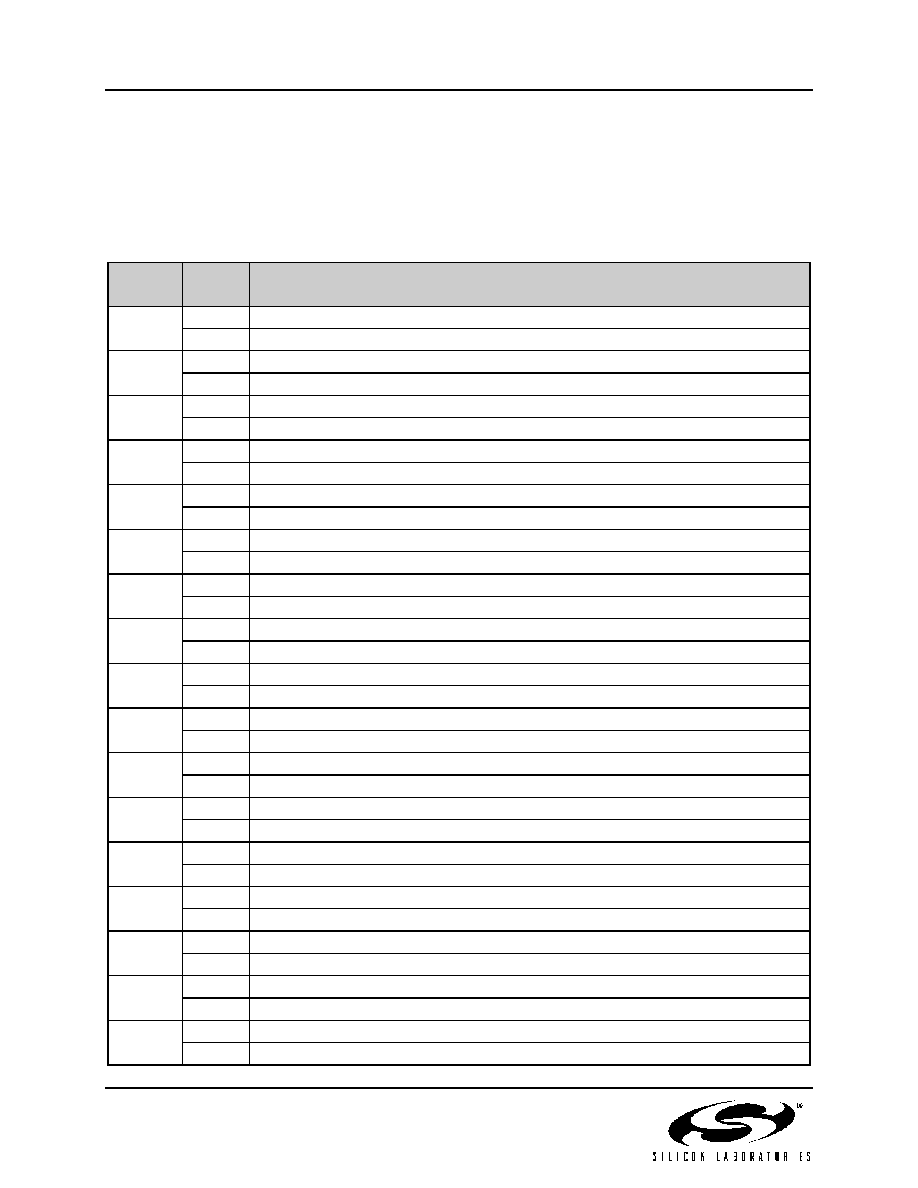
Table 21.1. Boundary Data Register Bit Definitions
EXTEST provides access to both capture and update actions, while Sample only performs a capture.
Bit
Action
Target
Capture
Reset Enable from MCU
0
Update
Reset Enable to /RST pin
Capture
Reset input from /RST pin
1
Update
Reset output to /RST pin
Capture
External Clock from XTAL1 pin
2
Update
Not used
Capture
Weak pullup enable from MCU
3
Update
Weak pullup enable to Port Pins
Capture
SFR Address Bus bit from CIP-51 (e.g. Bit4=SFRA0, Bit5=SFRA1…)
4-11
Update
SFR Address Bus bit to SFR Address Bus (e.g. Bit4=XSFRA0, Bit5=XSFRA1)
Capture
SFR Data Bus bit read from SFR (e.g. Bit12=SFRD0, Bit13=SFRD1…)
12-19
Update
SFR Data Bus bit written to SFR (e.g. Bit12=SFRD0, Bit13=SFRD1…)
Capture
SFR Write Strobe from CIP-51
20
Update
SFR Write Strobe to SFR Bus
Capture
SFR Read Strobe from CIP-51
21
Update
SFR Read Strobe to SFR Bus
Capture
SFR Read/Modify/Write Strobe from CIP-51
22
Update
SFR Read/Modify/Write Strobe to SFR Bus
Capture
P0.n output enable from MCU (e.g. Bit23=P0.0, Bit25=P0.1, etc.)
23,25,27,29,
31,33,35,37
Update
P0.n output enable to pin (e.g. Bit23=P0.0oe, Bit25=P0.1oe, etc.)
Capture
P0.n input from pin (e.g. Bit24=P0.0, Bit26=P0.1, etc.)
24,26,28,30,
32,34,36,38
Update
P0.n output to pin (e.g. Bit24=P0.0, Bit26=P0.1, etc.)
Capture
P1.n output enable from MCU (e.g. Bit39=P1.0, Bit41=P1.1, etc.)
39,41,43,45,
47,49,51,53
Update
P1.n output enable to pin (e.g. Bit39=P1.0oe, Bit41=P1.1oe, etc.)
Capture
P1.n input from pin (e.g. Bit40=P1.0, Bit42=P1.1, etc.)
40,42,44,46,
48,50,52,54
Update
P1.n output to pin (e.g. Bit40=P1.0, Bit42=P1.1, etc.)
Capture
P2.n output enable from MCU (e.g. Bit55=P2.0, Bit57=P2.1, etc.)
55,57,59,61,
63,65,67,69
Update
P2.n output enable to pin (e.g. Bit55=P2.0oe, Bit57=P2.1oe, etc.)
Capture
P2.n input from pin (e.g. Bit56=P2.0, Bit58=P2.1, etc.)
56,58,60,62,
64,66,68,70
Update
P2.n output to pin (e.g. Bit56=P2.0, Bit58=P2.1, etc.)
Capture
P3.n output enable from MCU (e.g. Bit71=P3.0, Bit73=P3.1, etc.)
71,73,75,77,
79,81,83,85
Update
P3.n output enable to pin (e.g. Bit71=P3.0oe, Bit73=P3.1oe, etc.)
Capture
P3.n input from pin (e.g. Bit72=P3.0, Bit74=P3.1, etc.)
72,74,76,78,
80,82,84,86
Update
P3.n output to pin (e.g. Bit72=P3.0, Bit74=P3.1, etc.)
165
Rev. 1.7
相關(guān)PDF資料 |
PDF描述 |
|---|---|
| ISC1210ER3R3J | INDUCTOR WW 3.3UH 5% 1210 |
| RP15-4812DF/P-HC | CONV DC/DC 15W 36-75VIN +/-12V |
| ISC1210ER2R7J | INDUCTOR WW 2.7UH 5% 1210 |
| ISC1210ER2R2J | INDUCTOR WW 2.2UH 5% 1210 |
| GSM06DRKF | CONN EDGECARD 12POS DIP .156 SLD |
相關(guān)代理商/技術(shù)參數(shù) |
參數(shù)描述 |
|---|---|
| C8051F011 | 功能描述:8位微控制器 -MCU 32KB 10ADC RoHS:否 制造商:Silicon Labs 核心:8051 處理器系列:C8051F39x 數(shù)據(jù)總線寬度:8 bit 最大時鐘頻率:50 MHz 程序存儲器大小:16 KB 數(shù)據(jù) RAM 大小:1 KB 片上 ADC:Yes 工作電源電壓:1.8 V to 3.6 V 工作溫度范圍:- 40 C to + 105 C 封裝 / 箱體:QFN-20 安裝風格:SMD/SMT |
| C8051F011-GQ | 功能描述:8位微控制器 -MCU 32KB 10ADC 48P MCU RoHS:否 制造商:Silicon Labs 核心:8051 處理器系列:C8051F39x 數(shù)據(jù)總線寬度:8 bit 最大時鐘頻率:50 MHz 程序存儲器大小:16 KB 數(shù)據(jù) RAM 大小:1 KB 片上 ADC:Yes 工作電源電壓:1.8 V to 3.6 V 工作溫度范圍:- 40 C to + 105 C 封裝 / 箱體:QFN-20 安裝風格:SMD/SMT |
| C8051F011-GQR | 功能描述:8位微控制器 -MCU 32KB 10ADC 48Pin MCU Tape and Reel RoHS:否 制造商:Silicon Labs 核心:8051 處理器系列:C8051F39x 數(shù)據(jù)總線寬度:8 bit 最大時鐘頻率:50 MHz 程序存儲器大小:16 KB 數(shù)據(jù) RAM 大小:1 KB 片上 ADC:Yes 工作電源電壓:1.8 V to 3.6 V 工作溫度范圍:- 40 C to + 105 C 封裝 / 箱體:QFN-20 安裝風格:SMD/SMT |
| C8051F011R | 功能描述:8位微控制器 -MCU C 10Bit 48Pin RoHS:否 制造商:Silicon Labs 核心:8051 處理器系列:C8051F39x 數(shù)據(jù)總線寬度:8 bit 最大時鐘頻率:50 MHz 程序存儲器大小:16 KB 數(shù)據(jù) RAM 大小:1 KB 片上 ADC:Yes 工作電源電壓:1.8 V to 3.6 V 工作溫度范圍:- 40 C to + 105 C 封裝 / 箱體:QFN-20 安裝風格:SMD/SMT |
| C8051F012 | 功能描述:8位微控制器 -MCU 32KB 10ADC RoHS:否 制造商:Silicon Labs 核心:8051 處理器系列:C8051F39x 數(shù)據(jù)總線寬度:8 bit 最大時鐘頻率:50 MHz 程序存儲器大小:16 KB 數(shù)據(jù) RAM 大小:1 KB 片上 ADC:Yes 工作電源電壓:1.8 V to 3.6 V 工作溫度范圍:- 40 C to + 105 C 封裝 / 箱體:QFN-20 安裝風格:SMD/SMT |
發(fā)布緊急采購,3分鐘左右您將得到回復。