- 您現(xiàn)在的位置:買賣IC網(wǎng) > PDF目錄374126 > C470UT200-Sxxxx (Cree, Inc.) Cree㈢ UltraThin⑩ LED PDF資料下載
參數(shù)資料
| 型號: | C470UT200-Sxxxx |
| 廠商: | Cree, Inc. |
| 英文描述: | Cree㈢ UltraThin⑩ LED |
| 中文描述: | Cree公司的LED㈢超薄⑩ |
| 文件頁數(shù): | 2/5頁 |
| 文件大小: | 282K |
| 代理商: | C470UT200-SXXXX |
Copyright 2006 Cree, Inc. All rights reserved. The information in this document is subject to change without notice. Cree, the
Cree logo and GSiC are registered trademarks, and UltraThin and UT are trademarks of Cree, Inc.
2
CPR3DE Rev. -
Cree, Inc.
4600 Silicon Drive
Durham, NC 27703
USA Tel: +1.919.313.5300
www.cree.com
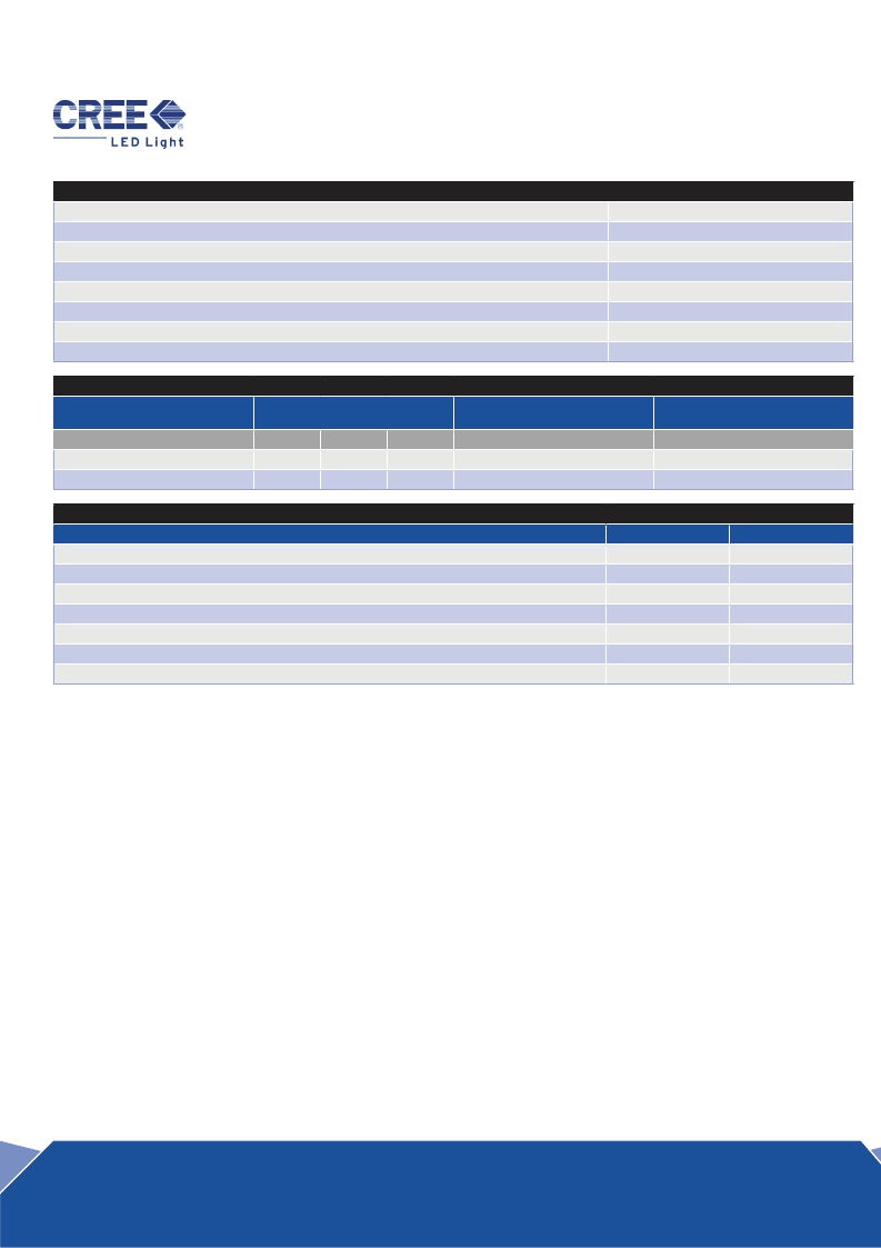
Maximum Ratings at T
A
= 25°C
Notes &3
DC Forward Current
C
xxx
UT200-S
xxxx
30 mA
Peak Forward Current (1/10 duty cycle @ 1 kHz)
100 mA
LED Junction Temperature
125°C
Reverse Voltage
5 V
Operating Temperature Range
-40°C to +100°C
Storage Temperature Range
-40°C to +100°C
Electrostatic Discharge Threshold (HBM)
Note 2
1000 V
Electrostatic Discharge Classification (MIL-STD-883E)
Note 2
Class 2
Typical Electrical/Optical Characteristics at T
A
= 25°C, If = 5 mA
Note 3
Part Number
Forward Voltage (V
f
, V)
Reverse Current
[I(Vr=5 V), μA]
Full Width Half Max
(
λ
D
, nm)
Min.
Typ.
Max.
Max.
Typ.
C460UT200-Sxxxx
2.7
2.9
3.1
2
21
C470UT200-Sxxxx
2.7
2.9
3.1
2
22
Mechanical Specifications
C
xxx
UT200-S
xxxx
Description
Dimension
Tolerance
P-N Junction Area (μm)
150 x 150
± 25
Top Area (μm)
200 x 200
± 25
Bottom Area (Substrate) (μm)
115 x 115
± 25
Chip Thickness (μm)
85
± 10
Au Bond Pad Diameter (μm)
90
-5, +15
Au Bond Pad Thickness (μm)
1.2
± 0.5
Back Contact Metal Area (μm)
80 x 80
± 25
Notes:
1.
Maximum ratings are package dependent. The above ratings were determined using a T-1 3/4 package (with Hysol OS4000
epoxy) for characterization. Ratings for other packages may differ. The forward currents (DC and Peak) are not limited by the die
but by the effect of the LED junction temperature on the package. The junction temperature limit of 125°C is a limit of the T-1
3/4 package; junction temperature should be characterized in a specific package to determine limitations. Assembly processing
temperature must not exceed 325°C (< 5 seconds).
Product resistance to electrostatic discharge (ESD) according to the HBM is measured by simulating ESD using a rapid avalanche
energy test (RAET). The RAET procedures are designed to approximate the minimum ESD ratings shown. The ESD classification of
Class 2 is based on sample testing according to MIL-STD-883E.
All products conform to the listed minimum and maximum specifications for electrical and optical characteristics when assembled
and operated at 5 mA within the maximum ratings shown above. Efficiency decreases at higher currents. Typical values given
are within the range of average values expected by manufacturer in large quantities and are provided for information only. All
measurements were made using lamps in T-1 3/4 packages (with Hysol OS4000 epoxy). Optical characteristics measured in an
integrating sphere using Illuminance E.
Caution: To obtain optimum output efficiency, the amount of epoxy used should be characterized based upon the specific
application.
2.
3.
4.
相關(guān)PDF資料 |
PDF描述 |
|---|---|
| C470UT230-S0002 | UltraThin⑩ LEDs |
| C470XB500-S3000-A | XBright㈢ Power Chip LED |
| C470XR260-Sxx00-A | XT⑩ Rectangular LEDs |
| C470XR260-Sxx00-x | XT⑩ Rectangular LEDs |
| C470XT290-Sxx00-x | XThin㈢ LEDs |
相關(guān)代理商/技術(shù)參數(shù) |
參數(shù)描述 |
|---|---|
| C470UT2200-0201 | 制造商:CREE 制造商全稱:Cree, Inc 功能描述:Small Chip 200 x 200 x 50 |
| C470UT2200-0202 | 制造商:CREE 制造商全稱:Cree, Inc 功能描述:Small Chip 200 x 200 x 50 |
| C470UT2200-0203 | 制造商:CREE 制造商全稱:Cree, Inc 功能描述:Small Chip 200 x 200 x 50 |
| C470UT2200-0204 | 制造商:CREE 制造商全稱:Cree, Inc 功能描述:Small Chip 200 x 200 x 50 |
| C470UT2200-0205 | 制造商:CREE 制造商全稱:Cree, Inc 功能描述:Small Chip 200 x 200 x 50 |
發(fā)布緊急采購,3分鐘左右您將得到回復(fù)。