- 您現(xiàn)在的位置:買賣IC網(wǎng) > PDF目錄374110 > C222G102D2CX5CA (KEMET Corporation) Ceramic Conformally Coated / Radial 'Standard & High Voltage Golden Max'; Capacitance [nom]: 10pF; Working Voltage (Vdc)[max]: 500V; Capacitance Tolerance: +/-5%; Dielectric: Multilayer Ceramic, Conformally Coated; Temperature Coefficient: C0G (NP0); Lead Style: Radial Leaded; Lead Dimensions: 0.200" Lead Spacing; Body Dimensions: 0.150" x 0.230" x 0.130"; Container: Tape & Reel; Qty per Container: 2500 PDF資料下載
參數(shù)資料
| 型號(hào): | C222G102D2CX5CA |
| 廠商: | KEMET Corporation |
| 英文描述: | Ceramic Conformally Coated / Radial 'Standard & High Voltage Golden Max'; Capacitance [nom]: 10pF; Working Voltage (Vdc)[max]: 500V; Capacitance Tolerance: +/-5%; Dielectric: Multilayer Ceramic, Conformally Coated; Temperature Coefficient: C0G (NP0); Lead Style: Radial Leaded; Lead Dimensions: 0.200" Lead Spacing; Body Dimensions: 0.150" x 0.230" x 0.130"; Container: Tape & Reel; Qty per Container: 2500 |
| 中文描述: | 背面軍事SPECIFCATIONS |
| 文件頁(yè)數(shù): | 15/40頁(yè) |
| 文件大?。?/td> | 580K |
| 代理商: | C222G102D2CX5CA |
第1頁(yè)第2頁(yè)第3頁(yè)第4頁(yè)第5頁(yè)第6頁(yè)第7頁(yè)第8頁(yè)第9頁(yè)第10頁(yè)第11頁(yè)第12頁(yè)第13頁(yè)第14頁(yè)當(dāng)前第15頁(yè)第16頁(yè)第17頁(yè)第18頁(yè)第19頁(yè)第20頁(yè)第21頁(yè)第22頁(yè)第23頁(yè)第24頁(yè)第25頁(yè)第26頁(yè)第27頁(yè)第28頁(yè)第29頁(yè)第30頁(yè)第31頁(yè)第32頁(yè)第33頁(yè)第34頁(yè)第35頁(yè)第36頁(yè)第37頁(yè)第38頁(yè)第39頁(yè)第40頁(yè)
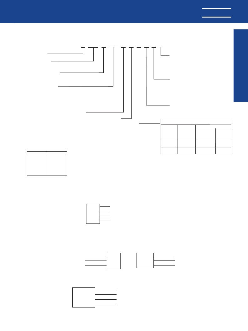
K
102
052
C
5
C
A
R
2
C
CERAMIC
*CASE SIZE
(See Table Below)
SPECIFICATION
Standard
C — Standard
CAPACITANCE
In picofarad code: First two digits are significant
figures and third is number of zeroes following
(except 9 indicates division by 10). Examples:
0.1
m
F = 100,000 pF = 104 and 9.1 pF = 919.
See tables for Standard Values.
CAPACITANCE TOLERANCE
Standard
M —
±
20%
K —
±
10%
J —
±
5%
D —
±
.5 pF
FAILURE RATE
A — Not Applicable (Std.)
INTERNAL CONSTRUCTION
5 — Standard
LEAD MATERIAL
C — Standard
WORKING
VOLTAGE
1 — 100
2 — 200
5 —
50
Others
H —
±
3%
G —
±
2%
F —
±
1%
TEMPERATURE CHARACTERISTIC
Cap. Change With Temp.
Measured
Without
DC Bias
Voltage
±
30
ppm/
°
C
KEMET
Designator
G
(Ultra
Stable)
R
(Stable)
EIA
Temp.
Range,
°
C
-55 to
+125
Equivalent
C0G
(NPO)
X7R
-55 to
+125
±
15%
Standard tolerances for each Series are
shown in the repetitive parts lists.
*CASE SIZES
RADIAL
AXIAL
C052
C114
C062
C124
C512
C192
C522
C202
C222
**
**Part Number Example: C052C102K2R5CA (14 digits – no spaces)
KEMET Electronics Corporation, P.O. Box 5928, Greenville, S.C. 29606, (864) 963-6300
15
KEMET
CERAMIC MOLDED/AXIAL & RADIAL - STANDARD
ORDERING INFORMATION
C
A
AXIAL CAPACITOR MARKINGS
STANDARD C114C, C124C, C192C, C202C & C222C
KC0G
101J
200V
0012
KEMET, Temperature Characteristic
Capacitance, Capacitance Tolerance
Voltage
Date Code
RADIAL CAPACITOR MARKINGS
C052C & C062C STANDARD MARKING
100V
K
0011
Voltage
KEMET
Date Code
BACK
C062
X7R
104K
FRONT
Style
Temperature Characteristic
Capacitance, Capacitance Tolerance
C512 & C522 STANDARD MARKING
KEMET
C512X7R
105K 50V
0032
KEMET
SIZE and Temperature Characteristic
Capacitance, Capacitance Tolerance, Voltage
Date Code
相關(guān)PDF資料 |
PDF描述 |
|---|---|
| C222G102D2CX5CM | MILITARY SPECIFCATIONS ON BACK |
| C222G102F1CJ5CR | MILITARY SPECIFCATIONS ON BACK |
| C222G102F1CK5CA | MILITARY SPECIFCATIONS ON BACK |
| C222G102F1CK5CM | MILITARY SPECIFCATIONS ON BACK |
| C222G102F1CK5CP | MILITARY SPECIFCATIONS ON BACK |
相關(guān)代理商/技術(shù)參數(shù) |
參數(shù)描述 |
|---|---|
| C222G102D2CX5CM | 制造商:KEMET 制造商全稱:Kemet Corporation 功能描述:MILITARY SPECIFCATIONS ON BACK |
| C222G102D2CX5CP | 制造商:KEMET 制造商全稱:Kemet Corporation 功能描述:MILITARY SPECIFCATIONS ON BACK |
| C222G102D2G5CA | 制造商:KEMET 制造商全稱:Kemet Corporation 功能描述:MILITARY SPECIFCATIONS ON BACK |
| C222G102D2G5CM | 制造商:KEMET 制造商全稱:Kemet Corporation 功能描述:MILITARY SPECIFCATIONS ON BACK |
| C222G102D2G5CP | 制造商:KEMET 制造商全稱:Kemet Corporation 功能描述:MILITARY SPECIFCATIONS ON BACK |
發(fā)布緊急采購(gòu),3分鐘左右您將得到回復(fù)。