- 您現(xiàn)在的位置:買(mǎi)賣(mài)IC網(wǎng) > PDF目錄369515 > BT169 (NXP Semiconductors N.V.) Thyristor logic level PDF資料下載
參數(shù)資料
| 型號(hào): | BT169 |
| 廠商: | NXP Semiconductors N.V. |
| 英文描述: | Thyristor logic level |
| 中文描述: | 晶閘管邏輯電平 |
| 文件頁(yè)數(shù): | 1/7頁(yè) |
| 文件大小: | 52K |
| 代理商: | BT169 |
Philips Semiconductors
Product specification
Thyristor
logic level
BT169W Series
GENERAL DESCRIPTION
QUICK REFERENCE DATA
Glass
thyristorinaplasticenvelope,suitable
forsurfacemounting,intendedforuse
in general purpose switching and
phase
control
applications.
device is intended to be interfaced
directly
to
microcontrollers,
integrated circuits and other low
power gate trigger circuits.
passivated,
sensitive
gate
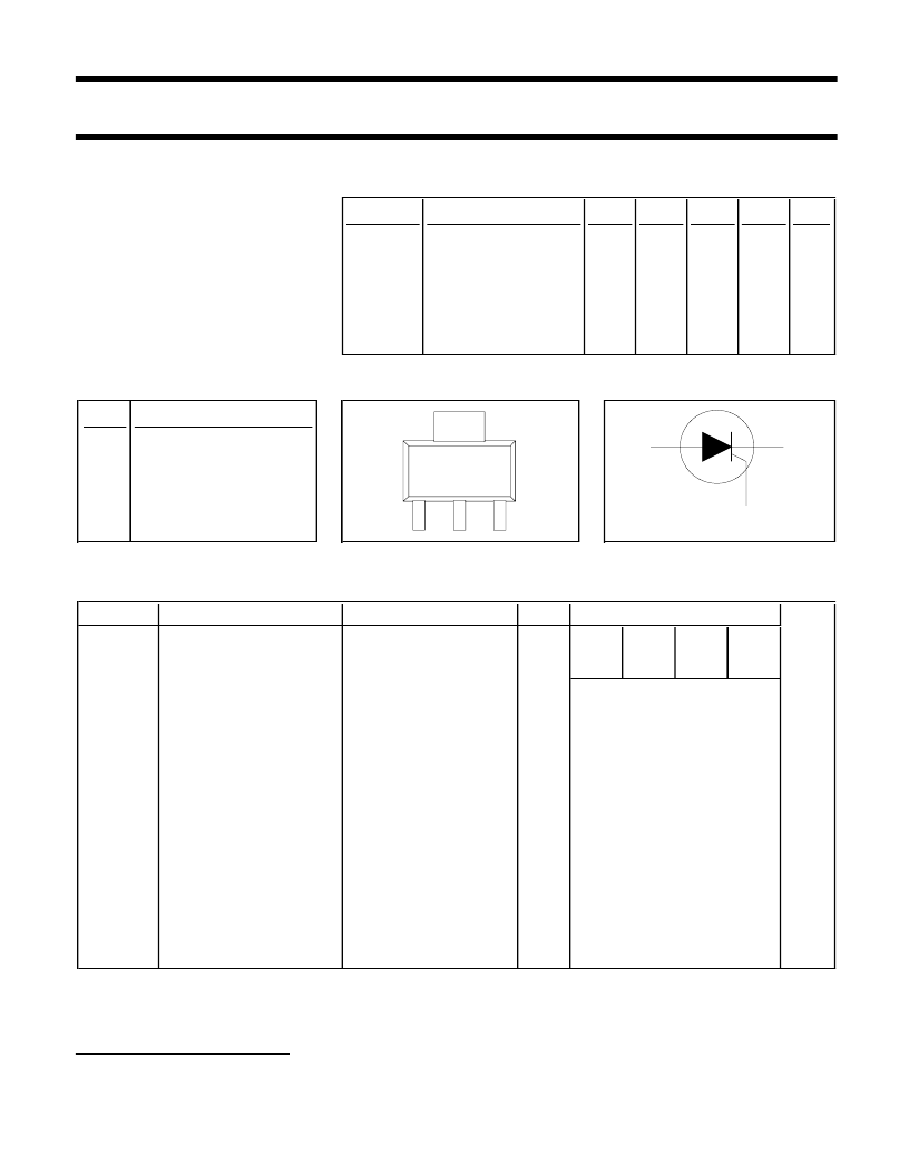
SYMBOL
PARAMETER
MAX.
MAX.
MAX.
MAX. UNIT
BT169
BW
200
DW
400
EW
500
GW
600
V
DRM
,
V
RRM
I
T(AV)
Repetitive peak
off-state voltages
Average on-state
current
RMS on-state current
Non-repetitive peak
on-state current
V
This
0.5
0.5
0.5
0.5
A
logic
I
T(RMS)
I
TSM
0.8
8
0.8
8
0.8
8
0.8
8
A
A
PINNING - SOT223
PIN CONFIGURATION
SYMBOL
PIN
DESCRIPTION
1
cathode
2
anode
3
gate
tab
anode
LIMITING VALUES
Limiting values in accordance with the Absolute Maximum System (IEC 134).
SYMBOL
PARAMETER
CONDITIONS
MIN.
MAX.
UNIT
B
D
E
G
V
DRM
, V
RRM
Repetitive peak off-state
voltages
I
T(AV)
Average on-state current
-
200
1
400
1
500
1
600
1
V
half sine wave;
T
≤
112 C
all conduction angles
half sine wave;
T
= 25 C prior to surge
t = 10 ms
t = 8.3 ms
t = 10 ms
I
TM
= 2 A; I
= 10 mA;
dI
G
/dt = 100 mA/
μ
s
-
0.63
A
I
T(RMS)
I
TSM
RMS on-state current
Non-repetitive peak
on-state current
-
1
A
-
-
-
-
8
9
A
A
I
2
t
dI
T
/dt
I
2
t for fusing
Repetitive rate of rise of
on-state current after
triggering
Peak gate current
Peak gate voltage
Peak reverse gate voltage
Peak gate power
Average gate power
Storage temperature
Operating junction
temperature
0.32
50
A
2
s
A/
μ
s
I
GM
V
GM
V
RGM
P
GM
P
G(AV)
T
stg
T
j
-
-
-
-
-
1
5
5
2
A
V
V
W
W
C
C
over any 20 ms period
0.1
150
125
-40
-
a
k
g
4
1
2
3
1
Although not recommended, off-state voltages up to 800V may be applied without damage, but the thyristor may
switch to the on-state. The rate of rise of current should not exceed 15 A/
μ
s.
September 1997
1
Rev 1.200
相關(guān)PDF資料 |
PDF描述 |
|---|---|
| BT169BW | Thyristor logic level |
| BT169DW | Thyristor logic level |
| BT169EW | Thyristor logic level |
| BT169W | Thyristor logic level |
| BT169_SERIES | Thyristors logic level |
相關(guān)代理商/技術(shù)參數(shù) |
參數(shù)描述 |
|---|---|
| BT169_08 | 制造商:UTC-IC 制造商全稱:UTC-IC 功能描述:SCRS |
| BT169_SERIES | 制造商:未知廠家 制造商全稱:未知廠家 功能描述:Thyristors logic level |
| BT16952DGG | 制造商:PHILIPS 制造商全稱:NXP Semiconductors 功能描述:16-bit registered transceiver 3-State |
| BT16952DL | 制造商:PHILIPS 制造商全稱:NXP Semiconductors 功能描述:16-bit registered transceiver 3-State |
| BT169B | 制造商:NXP Semiconductors 功能描述:Thyristor SCR 200V 9A 3-Pin SPT |
發(fā)布緊急采購(gòu),3分鐘左右您將得到回復(fù)。