- 您現在的位置:買賣IC網 > PDF目錄352721 > BS616LV2017EIG70 (BRILLIANCE SEMICONDUCTOR, INC.) Very Low Power/Voltage CMOS SRAM 128K X 16 bit PDF資料下載
參數資料
| 型號: | BS616LV2017EIG70 |
| 廠商: | BRILLIANCE SEMICONDUCTOR, INC. |
| 元件分類: | DRAM |
| 英文描述: | Very Low Power/Voltage CMOS SRAM 128K X 16 bit |
| 中文描述: | 非常低功率/電壓CMOS SRAM的128K的× 16位 |
| 文件頁數: | 1/8頁 |
| 文件大小: | 255K |
| 代理商: | BS616LV2017EIG70 |
Revision 2.1
Jan.
2004
1
R0201-BS616LV1611
Very Low Power/Voltage CMOS SRAM
1M X 16 bit
(Dual CE Pins)
The BS616LV1611 is a high performance, very low power CMOS Static
Random Access Memory organized as 1,048,576 words by 16 bits and
operates from a wide range of 2.4V to 5.5V supply voltage.
Advanced CMOS technology and circuit techniques provide both high
speed and low power features with a typical CMOS standby current
of 3.0uA at 3V/25oC and maximum access time of 55ns at 3.0V/85oC.
Easy memory expansion is provided by an active LOW chip enable(CE1)
, active HIGH chip enable (CE2), active LOW output enable(OE) and
three-state output drivers.
The BS616LV1611 has an automatic power down feature, reducing the
power consumption significantly when chip is deselected.
The BS616LV1611 is available in 48-pin BGA package.
DESCRIPTION
FEATURES
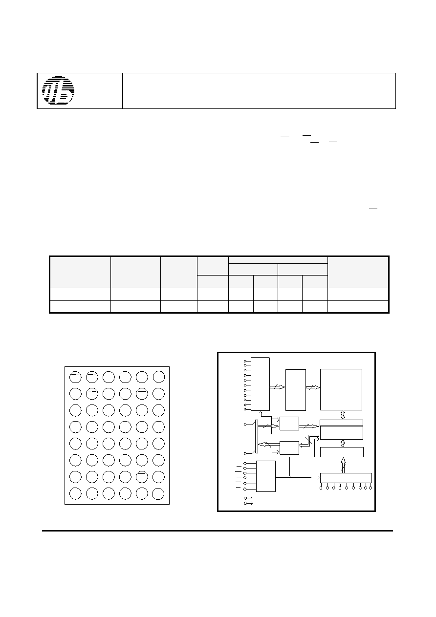
BLOCK DIAGRAM
PRODUCT FAMILY
PIN CONFIGURATIONS
Brilliance Semiconductor, Inc. reserves the right to modify document contents without notice.
BS616LV1611
LB
OE
A0
A1
A2
CE2
D8
UB
A3
A4
CE1
D0
D9
D10
A5
A6
D1
D2
VSS
D11
A17
A7
D3
VCC
D12
A16
D4
VSS
D14
D13
A14
A15
D5
D6
D15
A19
.
A12
A13
WE
D7
A8
A9
A10
A11
NC
1
A
B
C
D
E
F
G
H
1
23456
NC
Wide Vcc operation voltage : 2.4~5.5V
Very low power consumption :
Vcc = 3.0V C-grade: 45mA (@55ns) operating current
I -grade: 46mA (@55ns) operating current
C-grade: 36mA (@70ns) operating current
I -grade: 37mA (@70ns) operating current
3.0uA (Typ.) CMOS standby current
Vcc = 5.0V C-grade: 113mA (@55ns) operating current
I -grade: 115mA (@55ns) operating current
C-grade: 90mA (@70ns) operating current
I -grade: 92mA (@70ns) operating current
15uA (Typ.) CMOS standby current
High speed access time :
-55
55ns
-70
70ns
Automatic power down when chip is deselected
Three state outputs and TTL compatible
POWER DISSIPATION
SPEED
(ns)
STANDBY
(ICCSB1, Max)
Operating
(ICC, Max)
PRODUCT FAMILY
OPERATING
TEMPERATURE
Vcc
RANGE
Vcc=3V
Vcc=5V
PKG TYPE
BS616LV1611FC
+0 O C to +70 O C
2.4V ~ 5.5V
55 / 70
10uA
110uA
36mA
90mA
BGA-48-0912
BS616LV1611FI
-40 O C to +85 O C
2.4V ~ 5.5V
55 / 70
20uA
220uA
37mA
92mA
BGA-48-0912
Row
Decoder
Memory Array
2048 x 8192
Column I/O
Write Driver
Sense Amp
Column Decoder
Data
Buffer
Output
A9 A8 A7
Data
Buffer
Input
Control
Vss
Vcc
OE
WE
CE1
D15
D0
A0
A13
A14
A15
A1
A2
16
18
512
8192
2048
22
A17
A16
A10
A12
A6
A11
A3
Address
Input
Buffer
A5
Address Input Buffer
.
UB
.
LB
A4
A18
CE2
48-Ball CSP top View
BSI
Fully static operation
Data retention supply voltage as low as 1.5V
Easy expansion with CE2,CE1 and OE options
I/O Configuration x8/x16 selectable by LB and UB pin
55ns : 3.0~5.5V
70ns : 2.7~5.5V
Vcc=3V
Vcc=5V
70ns
A19
相關PDF資料 |
PDF描述 |
|---|---|
| BS616LV2017EIP70 | Very Low Power/Voltage CMOS SRAM 128K X 16 bit |
| BS616LV2018 | LM4946 ? Output Capacitor-Less Audio Subsystem with Programmable National 3D; Package: LLP; No of Pins: 24 |
| BS616LV2018AC | LM4946 ? Output Capacitor-Less Audio Subsystem with Programmable National 3D |
| BS616LV2018AI | LM4946 ? Output Capacitor-Less Audio Subsystem with Programmable National 3D; Package: LLP; No of Pins: 24 |
| BS616LV2018DC | LM4946 ? Output Capacitor-Less Audio Subsystem with Programmable National 3D; Package: MICRO SMD; No of Pins: 25 |
相關代理商/技術參數 |
參數描述 |
|---|---|
| BS616LV2017EIP55 | 制造商:BSI 制造商全稱:Brilliance Semiconductor 功能描述:Very Low Power/Voltage CMOS SRAM 128K X 16 bit |
| BS616LV2017EIP70 | 制造商:BSI 制造商全稱:Brilliance Semiconductor 功能描述:Very Low Power/Voltage CMOS SRAM 128K X 16 bit |
| BS616LV2018 | 制造商:BSI 制造商全稱:Brilliance Semiconductor 功能描述:Very Low Power/Voltage CMOS SRAM 128K X 16 bit |
| BS616LV2018AC | 制造商:BSI 制造商全稱:Brilliance Semiconductor 功能描述:Very Low Power/Voltage CMOS SRAM 128K X 16 bit |
| BS616LV2018AI | 制造商:BSI 制造商全稱:Brilliance Semiconductor 功能描述:Very Low Power/Voltage CMOS SRAM 128K X 16 bit |
發(fā)布緊急采購,3分鐘左右您將得到回復。