- 您現(xiàn)在的位置:買賣IC網(wǎng) > PDF目錄384151 > BP5034D5 (Rohm CO.,LTD.) AC/DC converter PDF資料下載
參數(shù)資料
| 型號: | BP5034D5 |
| 廠商: | Rohm CO.,LTD. |
| 英文描述: | AC/DC converter |
| 中文描述: | AC / DC變換器 |
| 文件頁數(shù): | 1/3頁 |
| 文件大小: | 37K |
| 代理商: | BP5034D5 |
BP5034D5
AC/DC converter
AC100V input, 5V/100mA output
Absolute Maximum Ratings
Input voltage
Output current
ESD endurance
Operating temperature range
Storage temperature range
Parameter
Symbol
Vi
Io
Vsurge
Topr
Tstg
Limits
195
100
2
20 ~
+
80
25 ~
+
85
Unit
V
mApk
kV
°
C
°
C
Unit
V
V
mA
V
V
Vp-p
%
2
2
1
Conditions
DC(80~138VAC)
Vi=141V, Io=50mA
Vi=141V
Vi=113~195V, Io=50mA
Vi=141V, Io=0~50mA
Vi=141V, Io=50mA
Vi=141V, Io=100mA
1 Maximum output current varies depending on ambient temperature ; please refer to derating curve.
2 Please refer to Load regulation, Conversion effciency.
Electrical Characteristics
Input voltage range
Output voltage
Output current
Line regulation
Load regulation
Output ripple voltage
Power conversion effciency
Parameter
Symbol
Vi
Vo
Io
Vr
Vl
Vp
η
Typ.
141
5.0
0.02
0.05
0.05
56
Max.
195
5.3
100
0.1
0.15
0.15
Min.
113
4.7
0
48
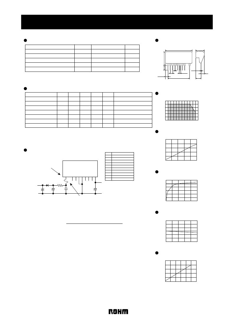
Load Regulation
(TLoad Regulation
°
C, Vi=141V)
5.3
5.2
5.1
5.0
4.9
4.8
4.7
20
Output Current Io(mA)
0
40
60
80
100
O
Conversion Efficiency
48% Min
Line
(Ta=25
°
C, Vi=141V)
60
50
40
30
20
10
0
0
20
Output Current Io(mA)
40
60
80
100
C
Surface Temperature Rising
Su(Ta=25
°
C, Vi=141V)
25
20
15
10
5
0
40
0
20
60
80
100
120
Output Current Io(mA)
T
T
°
C
Switching Frequency
(Ta=25
°
C, Vi=141V)
50
40
30
20
10
0
0
20
Output Current Io(mA)
40
60
80
100
S
Derating Curve
Derating Curve
Operation Range
120
100
80
60
40
20
0
0 10
-30-20 -10
20
40
30
80
70
60
50
90
Ambient Temperature Ta(
°
C)
O
Dimension (Unit :
mm
)
Application circuit
External components setting
FUSE: Fuse
C1: Capacitor for input
voltage smoothing
Please make sure to use quick acting fuse 0.5A
Capacitance : 3.3
μ
F~22
μ
F Rated voltage : 200V or higher
Ripple current is 0.13Arms above.
Capacitance : 0.1
μ
F~0.22
μ
F Rated voltage : 200V or higher
Film capacitor or ceramic capacitor. Reduce the noise terminal voltage.
The constant value should be evaluated in the set.
Capacitance : 100
μ
F~470
μ
F Rated voltage : 25V or higher,
ESR is 0.39
max. Ripple current is 0.1Arms above.
Output noise voltage is influenced.Please evaluate it in the actual set.
In the absolute maximum ratings, the reverse peak voltage should be
400V or higher, the average rectifying current should be 0.5A or higher,
and the peak surge current should be 20A or higher.
(Full-wave rectifier can be used in our part.)
10
~22
1/4W
Reduce the noise terminal voltage.The constant value should be evaluated
in set.
Varistor must be used. It protects this part from lightning surge and static
electricity.
C2: For noise terminal
voltage reduction
C3: Capacitor for Output
voltage smooting
D1: Rectifier diode
R1: For noise terminal
voltage reduction
ZNR: Varistor
Pin No.
1
2
3
4
5
6
7
8
9
10
Function
Output terminal Vo(5V)
N.C.
N.C.
N.C.
COMMON
COMMON
N.C.
N.C.
Not used
Input terminal Vi(141VDC)
For acutual usage, Please kindly evaluate and confirm our part mounted in your product,
Especially, Please make sure to confirm whether the load current exceed Max. rated current
by using the current probe.
BP5034D5
Please note that pin No.10
side is input.
Be sure to use fuse for safety.
+
5V
Output
Input
AC100V
50Hz/60Hz
100
μ
F/50V
0.1
μ
F
C2
0.5A
1
10
8 7 6 5 4 3 2
+
+
10
μ
F/250V
C1
ZNR
220V
R1
10
1/4W
D1
1SR35
400A
C3
1
M
4
±
1
28.2MAX.
10.0MAX.
3.5MAX.
6.5MAX.
2.54
×
9=22.86
1 2 3 4 5 6 7 8 10
0.5
±
0.1
P=2.54
±
0.2
1.3
±
0.2
0.25
±
0.05
3.25MAX
1/2
相關(guān)PDF資料 |
PDF描述 |
|---|---|
| BP5042-15 | AC/DC CONVERTER |
| BP5045A | AC/DC CONVERTER |
| BP5047A24 | AC220V input, 24V/150mA output |
| BP5061-5 | Circular Connector; MIL SPEC:MIL-C-26482, Series I, Solder; Body Material:Aluminum; Series:PT06; No. of Contacts:8; Connector Shell Size:12; Connecting Termination:Solder; Circular Shell Style:Straight Plug; Body Style:Straight |
| BP5065C | AC/DC converter AC100V input, −12V/90mA output |
相關(guān)代理商/技術(shù)參數(shù) |
參數(shù)描述 |
|---|---|
| BP5034D5_10 | 制造商:ROHM 制造商全稱:Rohm 功能描述:Non-Isolated AC/DC Converter |
| BP5035 | 制造商:ROHM 制造商全稱:Rohm 功能描述:AC / DC converter unit |
| BP5035-5 | 制造商:未知廠家 制造商全稱:未知廠家 功能描述:Analog IC |
| BP5035A12 | 功能描述:交流/直流開關(guān)轉(zhuǎn)換器 AC/DC -12V RoHS:否 制造商:STMicroelectronics 輸出電壓:800 V 輸入/電源電壓(最大值):23.5 V 輸入/電源電壓(最小值):11.5 V 開關(guān)頻率:115 kHz 電源電流:1.6 mA 工作溫度范圍:- 40 C to + 150 C 安裝風(fēng)格:SMD/SMT 封裝 / 箱體:SSO-10 封裝:Reel |
| BP5035A5 | 功能描述:交流/直流開關(guān)轉(zhuǎn)換器 IC -5V 200MA RoHS:否 制造商:STMicroelectronics 輸出電壓:800 V 輸入/電源電壓(最大值):23.5 V 輸入/電源電壓(最小值):11.5 V 開關(guān)頻率:115 kHz 電源電流:1.6 mA 工作溫度范圍:- 40 C to + 150 C 安裝風(fēng)格:SMD/SMT 封裝 / 箱體:SSO-10 封裝:Reel |
發(fā)布緊急采購,3分鐘左右您將得到回復(fù)。