- 您現(xiàn)在的位置:買賣IC網(wǎng) > PDF目錄357617 > BMA0218LA1 (MITEQ INC) 2000 MHz - 18000 MHz RF/MICROWAVE BIPHASE MODULATOR PDF資料下載
參數(shù)資料
| 型號: | BMA0218LA1 |
| 廠商: | MITEQ INC |
| 元件分類: | 調(diào)制器/解調(diào)器 |
| 英文描述: | 2000 MHz - 18000 MHz RF/MICROWAVE BIPHASE MODULATOR |
| 文件頁數(shù): | 3/3頁 |
| 文件大小: | 104K |
| 代理商: | BMA0218LA1 |
SSB UPCONVERTERS AND VECTOR MODULATORS/PHASE SHIFTERS
9
CARRIER DRIVEN
(LINEAR IF QAM)
(NOTE 1)
CARRIER
REJECTION
(dBc)
MODULATION DRIVEN
(LINEAR RF PM)
(NOTE 2)
CARRIER
REJECTION
(dBc)
FREQUENCY RANGE
RF
IN AND OUT
(GHz)
IF
SIDEBAND
REJECTION
(dBc)
SIDEBAND
REJECTION
(Typ./Min.)
CONVERSION
LOSS
(Typ./Max.)
MODEL
NUMBER
(GHz)
(Note 3)
SSB UPCONVERTERS WITH INTERNAL IF HYBRIDS
OUTLINES
NOTES
SDM0501LC1
SDM0502LC1
SDM0102LC1
SDM0104LC1
SME0104LI1
SDM0204LC1
SM0208LC2
SME0208LI1
SMC0208LI1
SM0408LC2
SM0812LC2
SM0218LC1
SM0618LC2
SME0618HI1
SME0618LI1
SML0618LC2
SM1218LC2
SM0226LC1
0.5 – 1
0.5 – 2
1 – 2
1 – 4
1 – 4
2 – 4
2 – 8
2 – 8
2 – 8
4 – 8
8 – 12
2 – 18
6 – 18
6 – 18
6 – 18
6 – 18
12 – 18
2 – 26
DC – 0.5
DC – 0.5
DC – 0.5
DC – 0.5
DC – 0.5
DC – 0.5
DC – 0.5
DC – 0.5
DC – 0.5
DC – 0.5
DC – 0.5
DC – 0.5
DC – 0.5
DC – 0.5
DC – 0.5
DC – 1
DC – 1
DC – 0.5
25
25
25
30
30
30
20
20
30
25
25
12
12
N/A
20
40
15
15
18
18
20
20
30
20
20
30
25
24
23
18
18
N/A
28
23
15
15
33
33
35
34
35
35
25
25
35
30
30
25
25
25
25
N/A
20
20
25 / 15
25 / 15
25 / 15
25 / 15
35 / 27
20 / 18
20 / 18
35 / 27
25 / 23
24 / 20
23 / 20
18 / 15
20 / 18
28 / 25
28 / 25
N/A
23 / 20
18 /15
8 / 10
8 / 10
8 / 10
8 / 10
10 / 12
8 / 10
9 / 11
11 / 13
7 / 10
6 / 9
6 / 9
9.5 / 11
8 / 9
10 / 13
10 / 13
N/A
7 / 9
12 / 15
8
8
8
8
22
8
13
22
21
13
13
8
8
9
13
22
22
13
13
PIN diodes, 8
Schottky diodes, 8
LO = 1/2 RF
9
SME0618LI1AVC
SME0618LI1DIQ
* Contact factory for outline drawings.
6 – 18
6 – 18 TTL
DC – .01
N/A
N/A
N/A
N/A
30
30
30 / 25
30 / 25
12 / 15
10 / 13
*
*
Analog phase/vector
Digital phase/vector
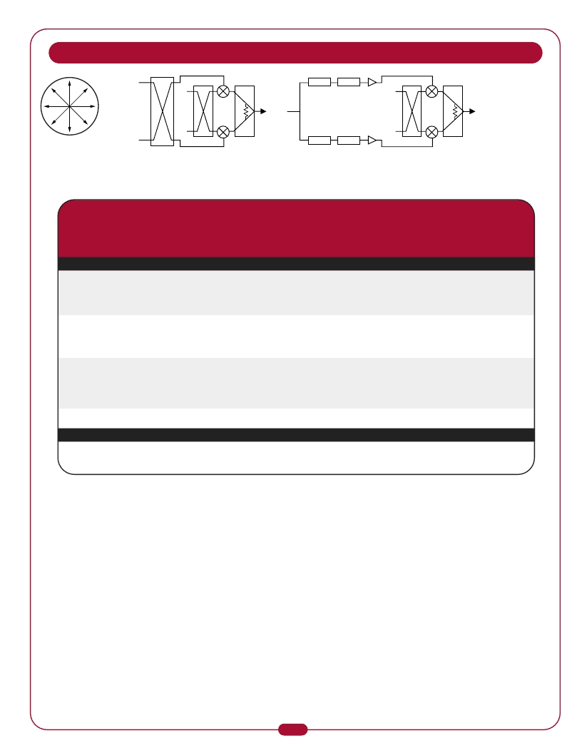
GENERAL
All modulators and SSB upconverters require that at least one of the input frequency bands (carrier or modulation) has sufficient power to turn on the
semiconductors used in the various designs (i.e., Schottky diodes or PIN diodes). All modulators yield a frequency spectrum that utilizes both sidebands
on either side of the output suppressed carrier. SSB upconverters employ an internal IF 90 degree hybrid to yield only 1 RF sideband output. This is
offset above or below the input LO by the IF frequency (test data is recorded for the upper sideband only). Schottky diode (standard) modulators have
the greatest speed and bandwidths, but yield RF output powers of typically less than 0 dBm. PIN diode (optional) designs can only be driven at
modulation rates of less than 30 MHz, but will yield output RF powers exceeding +5 dBm. PIN or Schottky modulators that vary only the RF carrier
phase, in many discrete steps or continuously, are referred to as phase shifters or frequency translators respectively. When output RF amplitude and
phase control is required, the device is usually called a vector modulator. For the latter device, phase accuracy is usually specified over a given
amplitude range (in dB). All MITEQ modulators can be driven in the carrier or modulation modes as explained below, but test data is only recorded in
the modulation driven mode.
SECTION 3 NOTES
Note 1:
Carrier driven:
transferred to the RF output envelope. A communication example would be directly modulating a microwave carrier with Gaussian shaped
I/Q digital pulses to minimize the channel bandwidth required.
Modulation driven: RF = 0 dBm, I/Q = +10 dBm or ±10 mA or TTL. Used when RF input has wide dynamic range, such as for military and
commercial Doppler frequency shift generation or corrections. If desired, the harmonic distortion of the relatively fixed and higher level I/Q
drive third order harmonics can be linearized by “resistance/diode” or digital “ROM” wave shaping techniques. The latter is often used in
vector modulator applications, such as in the model SME0618LI1DIQ design.
To specify the IF frequency for SSB upconverter usage, select from the following standard options and add to end of model number or
contact MITEQ:
Suffix A: 20–40 MHz, Suffix B: 40–80 MHz, Suffix C: 100–200 MHz, Suffix D: 500–1000 MHz, Suffix Q: I/Q inputs
Conversion loss (CL) is relative to lowest power input (f
, f
). All other outputs (including f
, are relative to the desired upper (f
+ f
) output.
Standard units with IF hybrids are aligned for upper sideband operation.
Last two characters in model number indicate standard outline number, see outline section.
Question and answer modulator application notes available, contact factory.
Hermetically sealed housing.
LO = +13 dBm, I/Q = 0 dBm. Used when any amplitude variation or pulse shape of the modulation must be accurately
Note 2:
Note 3:
Note 4:
Note 5:
Note 6:
Note 7:
Note 8:
For lower sideband or selectable sideband, contact MITEQ.
ANALOG OR DIGITALLY CONTROLLED VECTOR MODULATORS/PHASE SHIFTERS
fm
fo
fm
fo
ROM
D/A
ROM
D/A
SDM, SML-A...D
Single-Sideband Upconverter
LO and 1/2 LO
SMC, SME...AVC/DIQ
Analog/Digital, Phase/Amp Control
MPSK
相關(guān)PDF資料 |
PDF描述 |
|---|---|
| BML1206-220RK | 1 ELEMENT, 22 uH, FERRITE-CORE, GENERAL PURPOSE INDUCTOR, SMD |
| BML32163R3K | GENERAL PURPOSE INDUCTOR |
| BML32165R6K | GENERAL PURPOSE INDUCTOR |
| BNC-B-48 | INTERCONNECTION DEVICE |
| BNC5-J-C-HN-ST-BH1 | PANEL MOUNT, CABLE TERMINATED, FEMALE, BNC CONNECTOR, CRIMP SOLDER, JACK |
相關(guān)代理商/技術(shù)參數(shù) |
參數(shù)描述 |
|---|---|
| BMA-02-24-XX-N | 制造商:PCTEL 功能描述:ANTENNA UNIT |
| BMA-02-36-XX-N | 制造商:PCTEL 功能描述:ANTENNA UNIT |
| BMA10L | 制造商:未知廠家 制造商全稱:未知廠家 功能描述:IC-100W POWER AMP |
| BMA1101 | 功能描述:程序設(shè)計器配件 OTP Write Adapter RoHS:否 制造商:Lattice 產(chǎn)品:ispDOWNLOAD Cables 用于:In-system Programming |
| BMA1102 | 功能描述:程序設(shè)計器配件 OTP Write Adapter RoHS:否 制造商:Lattice 產(chǎn)品:ispDOWNLOAD Cables 用于:In-system Programming |
發(fā)布緊急采購,3分鐘左右您將得到回復(fù)。