- 您現(xiàn)在的位置:買賣IC網(wǎng) > PDF目錄4399 > AX500-1FG676I (Microsemi SoC)IC FPGA AXCELERATOR 500K 676FBGA PDF資料下載
參數(shù)資料
| 型號: | AX500-1FG676I |
| 廠商: | Microsemi SoC |
| 文件頁數(shù): | 260/262頁 |
| 文件大小: | 0K |
| 描述: | IC FPGA AXCELERATOR 500K 676FBGA |
| 標(biāo)準(zhǔn)包裝: | 40 |
| 系列: | Axcelerator |
| 邏輯元件/單元數(shù): | 5376 |
| RAM 位總計: | 73728 |
| 輸入/輸出數(shù): | 336 |
| 門數(shù): | 500000 |
| 電源電壓: | 1.425 V ~ 1.575 V |
| 安裝類型: | 表面貼裝 |
| 工作溫度: | -40°C ~ 85°C |
| 封裝/外殼: | 676-BGA |
| 供應(yīng)商設(shè)備封裝: | 676-FBGA(27x27) |
第1頁第2頁第3頁第4頁第5頁第6頁第7頁第8頁第9頁第10頁第11頁第12頁第13頁第14頁第15頁第16頁第17頁第18頁第19頁第20頁第21頁第22頁第23頁第24頁第25頁第26頁第27頁第28頁第29頁第30頁第31頁第32頁第33頁第34頁第35頁第36頁第37頁第38頁第39頁第40頁第41頁第42頁第43頁第44頁第45頁第46頁第47頁第48頁第49頁第50頁第51頁第52頁第53頁第54頁第55頁第56頁第57頁第58頁第59頁第60頁第61頁第62頁第63頁第64頁第65頁第66頁第67頁第68頁第69頁第70頁第71頁第72頁第73頁第74頁第75頁第76頁第77頁第78頁第79頁第80頁第81頁第82頁第83頁第84頁第85頁第86頁第87頁第88頁第89頁第90頁第91頁第92頁第93頁第94頁第95頁第96頁第97頁第98頁第99頁第100頁第101頁第102頁第103頁第104頁第105頁第106頁第107頁第108頁第109頁第110頁第111頁第112頁第113頁第114頁第115頁第116頁第117頁第118頁第119頁第120頁第121頁第122頁第123頁第124頁第125頁第126頁第127頁第128頁第129頁第130頁第131頁第132頁第133頁第134頁第135頁第136頁第137頁第138頁第139頁第140頁第141頁第142頁第143頁第144頁第145頁第146頁第147頁第148頁第149頁第150頁第151頁第152頁第153頁第154頁第155頁第156頁第157頁第158頁第159頁第160頁第161頁第162頁第163頁第164頁第165頁第166頁第167頁第168頁第169頁第170頁第171頁第172頁第173頁第174頁第175頁第176頁第177頁第178頁第179頁第180頁第181頁第182頁第183頁第184頁第185頁第186頁第187頁第188頁第189頁第190頁第191頁第192頁第193頁第194頁第195頁第196頁第197頁第198頁第199頁第200頁第201頁第202頁第203頁第204頁第205頁第206頁第207頁第208頁第209頁第210頁第211頁第212頁第213頁第214頁第215頁第216頁第217頁第218頁第219頁第220頁第221頁第222頁第223頁第224頁第225頁第226頁第227頁第228頁第229頁第230頁第231頁第232頁第233頁第234頁第235頁第236頁第237頁第238頁第239頁第240頁第241頁第242頁第243頁第244頁第245頁第246頁第247頁第248頁第249頁第250頁第251頁第252頁第253頁第254頁第255頁第256頁第257頁第258頁第259頁當(dāng)前第260頁第261頁第262頁
Axcelerator Family FPGAs
Re vi s i on 18
2 - 83
Sample Implementations
Frequency Synthesis
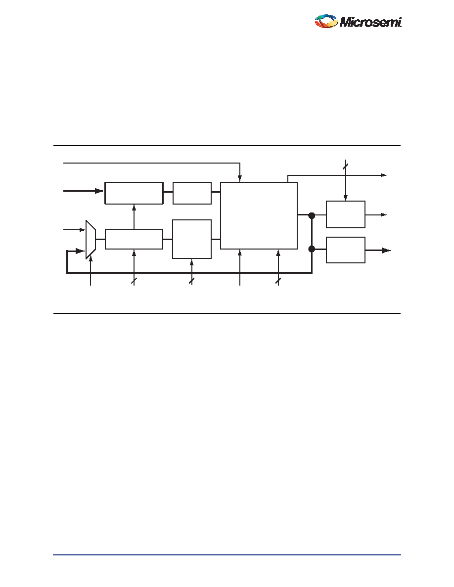
Figure 2-53 illustrates an example where the PLL is used to multiply a 155.5 MHz external clock up to
622 MHz. Note that the same PLL schematic could use an external 350 MHz clock, which is divided
down to 155 MHz by the FPGA internal logic.
Figure 2-54 illustrates the PLL using both dividers to synthesize a 133 MHz output clock from a 155 MHz
input reference clock. The input frequency of 155 MHz is multiplied by 6 and divided by 7, giving a CLK1
output frequency of 132.86 MHz. When dividers are used, a given ratio can be generated in multiple
ways, allowing the user to stay within the operating frequency ranges of the PLL.
Adjustable Clock Delay
Figure 2-55 illustrates using the PLL to delay the reference clock by employing one of the adjustable
delay lines. In this case, the output clock is delayed relative to the reference clock. Delaying the
reference clock relative to the output clock is accomplished by using the delay line in the feedback path.
Figure 2-53 Using the PLL 155.5 MHz In, 622 MHz Out
Delay Line
PLL
Delay Line
RefCLK
FB
/i
6
/j
6
CLK1
Power-Down
Lock
CLK2
FBMuxSel
5
DividerI
DelayLine
DividerJ
LowFreq
3
Osc
+4
155.5 MHz
622 MHz
/i Delay
Match
/j Delay
Match
相關(guān)PDF資料 |
PDF描述 |
|---|---|
| ACM36DTBN-S664 | CONN EDGECARD 72POS R/A .156 |
| AX500-1FGG676I | IC FPGA AXCELERATOR 500K 676FBGA |
| 24LC00/P | IC EEPROM 128BIT 400KHZ 8DIP |
| A54SX72A-FG484A | IC FPGA SX-A 108K 484-FBGA |
| AGLE600V2-FG484I | IC FPGA 1KB FLASH 600K 484-FBGA |
相關(guān)代理商/技術(shù)參數(shù) |
參數(shù)描述 |
|---|---|
| AX500-1FG676M | 制造商:Microsemi Corporation 功能描述:FPGA AXCELERATOR 286K GATES 5376 CELLS 763MHZ 0.15UM 1.5V 67 - Trays 制造商:Microsemi Corporation 功能描述:IC FPGA 336 I/O 676FBGA 制造商:Microsemi Corporation 功能描述:IC FPGA AXCELERATOR 500K 676FBGA |
| AX500-1FG896 | 制造商:ACTEL 制造商全稱:Actel Corporation 功能描述:Axcelerator Family FPGAs |
| AX500-1FG896B | 制造商:ACTEL 制造商全稱:Actel Corporation 功能描述:Axcelerator Family FPGAs |
| AX500-1FG896I | 制造商:ACTEL 制造商全稱:Actel Corporation 功能描述:Axcelerator Family FPGAs |
| AX500-1FG896M | 制造商:ACTEL 制造商全稱:Actel Corporation 功能描述:Axcelerator Family FPGAs |
發(fā)布緊急采購,3分鐘左右您將得到回復(fù)。