- 您現(xiàn)在的位置:買賣IC網(wǎng) > PDF目錄379701 > ATT3064-100J68I (Electronic Theatre Controls, Inc.) Field-Programmable Gate Arrays PDF資料下載
參數(shù)資料
| 型號(hào): | ATT3064-100J68I |
| 廠商: | Electronic Theatre Controls, Inc. |
| 元件分類: | FPGA |
| 英文描述: | Field-Programmable Gate Arrays |
| 中文描述: | 現(xiàn)場(chǎng)可編程門陣列 |
| 文件頁數(shù): | 18/80頁 |
| 文件大小: | 528K |
| 代理商: | ATT3064-100J68I |
第1頁第2頁第3頁第4頁第5頁第6頁第7頁第8頁第9頁第10頁第11頁第12頁第13頁第14頁第15頁第16頁第17頁當(dāng)前第18頁第19頁第20頁第21頁第22頁第23頁第24頁第25頁第26頁第27頁第28頁第29頁第30頁第31頁第32頁第33頁第34頁第35頁第36頁第37頁第38頁第39頁第40頁第41頁第42頁第43頁第44頁第45頁第46頁第47頁第48頁第49頁第50頁第51頁第52頁第53頁第54頁第55頁第56頁第57頁第58頁第59頁第60頁第61頁第62頁第63頁第64頁第65頁第66頁第67頁第68頁第69頁第70頁第71頁第72頁第73頁第74頁第75頁第76頁第77頁第78頁第79頁第80頁
Data Sheet
February 1997
ATT3000 Series Field-Programmable Gate Arrays
18
Lucent Technologies Inc.
Configuration
(continued)
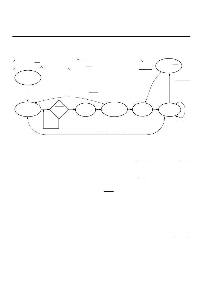
Figure 18. State Diagram of Configuration Process for Powerup and Reprogram
5-3110(F)
INITIALIZATION
POWER-ON
TIME DELAY
CLEAR
CONFIGURATION
MEMORY
YES
RESET
ACTIVE
NO
TEST
MODE PINS
CONFIGURATION
PROGRAM MODE
OPERATIONAL
MODE
START-UP
INIT = LOW
USER I/O PINS WITH HIGH-IMPEDANCE PULL-UP
HDC = HIGH
LDC = LOW
ACTIVE RESET
POWERDOWN
NO HDC, LDC
OR PULL-UP
INACTIVE
PWRDWN
ACTIVE RESET
OPERATES ON
USER LOGIC
LOW ON DONE/PROG AND RESET
ACTIVE
PWRDWN
Length count control allows a system of multiple
FPGAs in assorted sizes to begin operation in a syn-
chronized fashion. The configuration program gener-
ated by the
ORCA
Foundry Development System
begins with a preamble of 111111110010 (binary), fol-
lowed by a 24-bit length count representing the total
number of configuration clocks needed to complete
loading of the configuration program(s). The data fram-
ing is shown in Figure 19. All FPGAs connected in
series read and shift preamble and length count in (on
positive) and out (on negative) CCLK edges. An FPGA
which has received the preamble and length count then
presents a HIGH data out until it has intercepted the
appropriate number of data frames. When the configu-
ration program memory of an FPGA is full and the
length count does not compare, the FPGA shifts any
additional data through, as it did for preamble and
length count.
When the FPGA configuration memory is full and the
length count compares, the FPGA will execute a syn-
chronous start-up sequence and become operational
(see Figure 20 on page 20). Two CCLK cycles after the
completion of loading configuration data, the user
I/O pins are enabled as configured. As selected in
ORCA
Foundry, the internal user-logic reset is released
either one clock cycle before or after the I/O pins
become active. A similar timing selection is program-
mable for the DONE/
PROG
output signal. DONE/
PROG
may also be programmed to be an open drain or
include a pull-up resistor to accommodate wired-
ANDing. The high during configuration (HDC) and low
during configuration (
LDC
) are two user I/O pins which
are driven active when an FPGA is in initialization,
clear, or configure states. These signals and DONE/
PROG
provide for control of external logic signals such
as reset, bus enable, or PROM enable during
configuration.
For parallel master configuration modes, these signals
provide PROM enable control and allow the data pins
to be shared with user logic signals.
User I/O inputs can be programmed to be either TTL or
CMOS compatible thresholds. At powerup, all inputs
have TTL thresholds and can change to CMOS thresh-
olds at the completion of configuration, if the user has
selected CMOS thresholds. The threshold of
PWRDWN
and the direct clock inputs are fixed at a CMOS level.
If the crystal oscillator is used, it will begin operation
before configuration is complete to allow time for
stabilization before it is connected to the internal
circuitry.
相關(guān)PDF資料 |
PDF描述 |
|---|---|
| ATT3064-100J84I | Field-Programmable Gate Arrays |
| ATT3064-100M132I | Field-Programmable Gate Arrays |
| ATT3064-100M44I | Field-Programmable Gate Arrays |
| ATT3064-100M68I | Field-Programmable Gate Arrays |
| ATT3064-100S132I | Field-Programmable Gate Arrays |
相關(guān)代理商/技術(shù)參數(shù) |
參數(shù)描述 |
|---|---|
| ATT3064-100J84I | 制造商:未知廠家 制造商全稱:未知廠家 功能描述:Field-Programmable Gate Arrays |
| ATT3064-100M132I | 制造商:未知廠家 制造商全稱:未知廠家 功能描述:Field-Programmable Gate Arrays |
| ATT3064-100M44I | 制造商:未知廠家 制造商全稱:未知廠家 功能描述:Field-Programmable Gate Arrays |
| ATT3064-100M68I | 制造商:未知廠家 制造商全稱:未知廠家 功能描述:Field-Programmable Gate Arrays |
| ATT3064-100M84 | 制造商:未知廠家 制造商全稱:未知廠家 功能描述:Field Programmable Gate Array (FPGA) |
發(fā)布緊急采購,3分鐘左右您將得到回復(fù)。