- 您現(xiàn)在的位置:買賣IC網(wǎng) > PDF目錄4358 > EP2AGX65DF25C4 (Altera)IC ARRIA II GX FPGA 65K 572FBGA PDF資料下載
參數(shù)資料
| 型號: | EP2AGX65DF25C4 |
| 廠商: | Altera |
| 文件頁數(shù): | 31/90頁 |
| 文件大?。?/td> | 0K |
| 描述: | IC ARRIA II GX FPGA 65K 572FBGA |
| 產(chǎn)品培訓模塊: | Three Reasons to Use FPGA's in Industrial Designs |
| 標準包裝: | 5 |
| 系列: | Arria II GX |
| LAB/CLB數(shù): | 2530 |
| 邏輯元件/單元數(shù): | 60214 |
| RAM 位總計: | 5371904 |
| 輸入/輸出數(shù): | 252 |
| 電源電壓: | 0.87 V ~ 0.93 V |
| 安裝類型: | 表面貼裝 |
| 工作溫度: | 0°C ~ 85°C |
| 封裝/外殼: | 572-FBGA |
| 供應商設(shè)備封裝: | 572-FBGA |
第1頁第2頁第3頁第4頁第5頁第6頁第7頁第8頁第9頁第10頁第11頁第12頁第13頁第14頁第15頁第16頁第17頁第18頁第19頁第20頁第21頁第22頁第23頁第24頁第25頁第26頁第27頁第28頁第29頁第30頁當前第31頁第32頁第33頁第34頁第35頁第36頁第37頁第38頁第39頁第40頁第41頁第42頁第43頁第44頁第45頁第46頁第47頁第48頁第49頁第50頁第51頁第52頁第53頁第54頁第55頁第56頁第57頁第58頁第59頁第60頁第61頁第62頁第63頁第64頁第65頁第66頁第67頁第68頁第69頁第70頁第71頁第72頁第73頁第74頁第75頁第76頁第77頁第78頁第79頁第80頁第81頁第82頁第83頁第84頁第85頁第86頁第87頁第88頁第89頁第90頁
Chapter 1: Device Datasheet for Arria II Devices
1–29
Switching Characteristics
December 2013
Altera Corporation
Transceiver Clocks
Calibration block clock
frequency (cal_blk_clk)
—
10
—
125
10
—
125
MHz
fixedclk
clock frequency
PCIe Receiver
Detect
—
125
—
125
—
MHz
reconfig_clk
clock
frequency
Dynamic
reconfiguration
clock frequency
2.5/
37.5
—50
2.5/
37.5
—50
MHz
Delta time between
reconfig_clks
——
—
2
—
2
ms
Transceiver block minimum
power-down
(gxb_powerdown) pulse
width
—1
—
1
—
s
Receiver
Supported I/O Standards
1.4-V PCML, 1.5-V PCML, 2.5-V PCML, LVPECL, and LVDS
Data rate (16)
—
600
—
6375
600
—
3750
Mbps
Absolute VMAX for a receiver
pin (6)
——
—
1.6
—
1.6
V
Operational VMAX for a
receiver pin
——
—
1.5
—
1.5
V
Absolute VMIN for a receiver
pin
—
-0.4
—
-0.4
—
V
Maximum peak-to-peak
differential input voltage VID
(diff p-p) before device
configuration
——
—
1.6
—
1.6
V
Maximum peak-to-peak
differential input voltage VID
(diff p-p) after device
configuration
VICM = 0.82 V
setting
—
2.7
—
2.7
V
VICM =1.1 V setting
—
1.6
—
1.6
V
Minimum differential eye
opening at receiver serial
input pins (8)
Data Rate =
600 Mbps to
5 Gbps
Equalization = 0
DC gain = 0 dB
100
—
165
—
mV
Data Rate > 5 Gbps
Equalization = 0
DC gain = 0 dB
165
—
165
—
mV
VICM
VICM = 0.82 V
setting
820 ± 10%
mV
VICM = 1.1 V setting
1100 ± 10%
mV
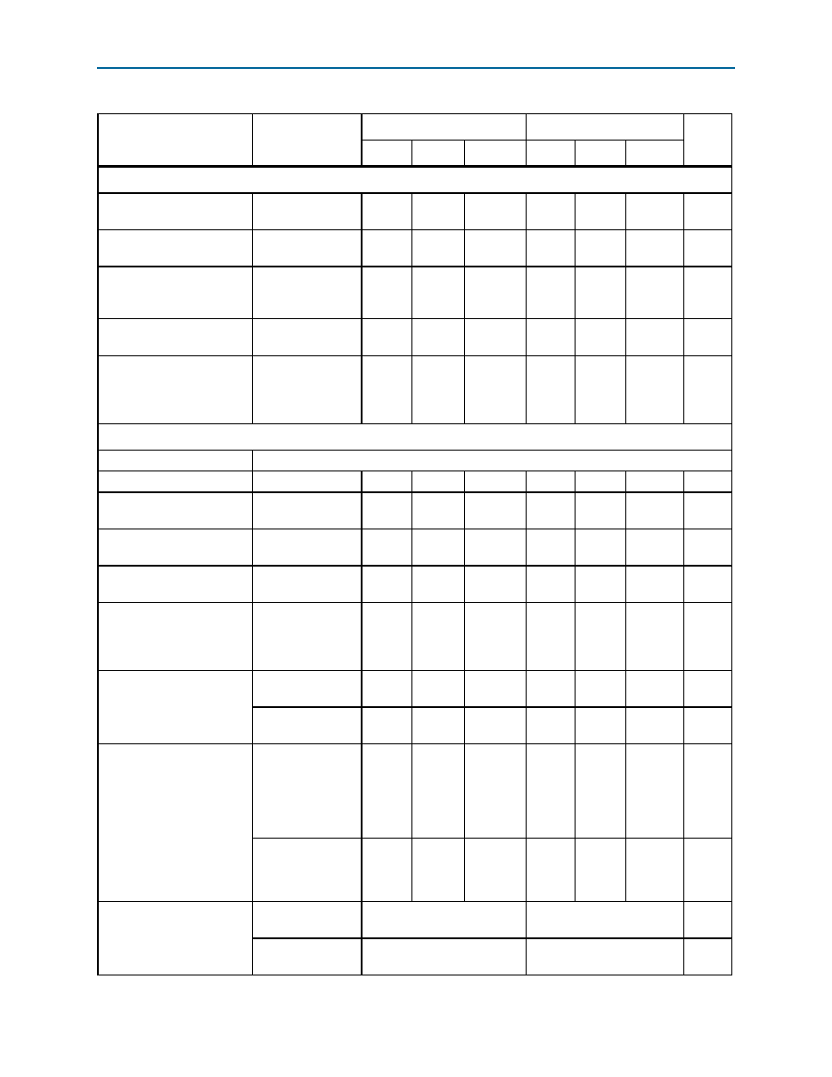
Table 1–35. Transceiver Specifications for Arria II GZ Devices (Part 2 of 5)
Symbol/
Description
Conditions
–C3 and –I3 (1)
–C4 and –I4
Unit
Min
Typ
Max
Min
Typ
Max
相關(guān)PDF資料 |
PDF描述 |
|---|---|
| EPF10K130EFC484-1 | IC FLEX 10KE FPGA 130K 484-FBGA |
| ACC49DRYH-S13 | CONN EDGECARD 98POS .100 EXTEND |
| APA750-BG456I | IC FPGA PROASIC+ 750K 456-PBGA |
| 180-026-273L030 | CONN DB26 FEMALE HD CRIMP NICKEL |
| AYM43DRSN-S288 | CONN EDGECARD 86POS .156 EXTEND |
相關(guān)代理商/技術(shù)參數(shù) |
參數(shù)描述 |
|---|---|
| EP2AGX65DF25C4N | 功能描述:FPGA - 現(xiàn)場可編程門陣列 FPGA - Arria II GX 2530 LABs 252 IOs RoHS:否 制造商:Altera Corporation 系列:Cyclone V E 柵極數(shù)量: 邏輯塊數(shù)量:943 內(nèi)嵌式塊RAM - EBR:1956 kbit 輸入/輸出端數(shù)量:128 最大工作頻率:800 MHz 工作電源電壓:1.1 V 最大工作溫度:+ 70 C 安裝風格:SMD/SMT 封裝 / 箱體:FBGA-256 |
| EP2AGX65DF25C5 | 功能描述:FPGA - 現(xiàn)場可編程門陣列 FPGA - Arria II GX 2530 LABs 252 IOs RoHS:否 制造商:Altera Corporation 系列:Cyclone V E 柵極數(shù)量: 邏輯塊數(shù)量:943 內(nèi)嵌式塊RAM - EBR:1956 kbit 輸入/輸出端數(shù)量:128 最大工作頻率:800 MHz 工作電源電壓:1.1 V 最大工作溫度:+ 70 C 安裝風格:SMD/SMT 封裝 / 箱體:FBGA-256 |
| EP2AGX65DF25C5N | 功能描述:FPGA - 現(xiàn)場可編程門陣列 FPGA - Arria II GX 2530 LABs 252 IOs RoHS:否 制造商:Altera Corporation 系列:Cyclone V E 柵極數(shù)量: 邏輯塊數(shù)量:943 內(nèi)嵌式塊RAM - EBR:1956 kbit 輸入/輸出端數(shù)量:128 最大工作頻率:800 MHz 工作電源電壓:1.1 V 最大工作溫度:+ 70 C 安裝風格:SMD/SMT 封裝 / 箱體:FBGA-256 |
| EP2AGX65DF25C6 | 功能描述:FPGA - 現(xiàn)場可編程門陣列 FPGA - Arria II GX 2530 LABs 252 IOs RoHS:否 制造商:Altera Corporation 系列:Cyclone V E 柵極數(shù)量: 邏輯塊數(shù)量:943 內(nèi)嵌式塊RAM - EBR:1956 kbit 輸入/輸出端數(shù)量:128 最大工作頻率:800 MHz 工作電源電壓:1.1 V 最大工作溫度:+ 70 C 安裝風格:SMD/SMT 封裝 / 箱體:FBGA-256 |
| EP2AGX65DF25C6ES | 制造商:Altera Corporation 功能描述:FPGA Arria |
發(fā)布緊急采購,3分鐘左右您將得到回復。