- 您現(xiàn)在的位置:買賣IC網(wǎng) > PDF目錄51298 > ASJD1200R045SY-EL/V (MICROSS COMPONENTS) 50 A, 1200 V, 0.045 ohm, N-CHANNEL, SiC, POWER, JFET, TO-257AA PDF資料下載
參數(shù)資料
| 型號: | ASJD1200R045SY-EL/V |
| 廠商: | MICROSS COMPONENTS |
| 元件分類: | JFETs |
| 英文描述: | 50 A, 1200 V, 0.045 ohm, N-CHANNEL, SiC, POWER, JFET, TO-257AA |
| 封裝: | HERMETIC SEALED, TO-257, 3 PIN |
| 文件頁數(shù): | 2/4頁 |
| 文件大?。?/td> | 162K |
| 代理商: | ASJD1200R045SY-EL/V |
SiC JFET
ASJD1200R045
ASJD1200R045
Rev. 0.0 12/10
Micross Components reserves the right to change products or specications without notice.
2
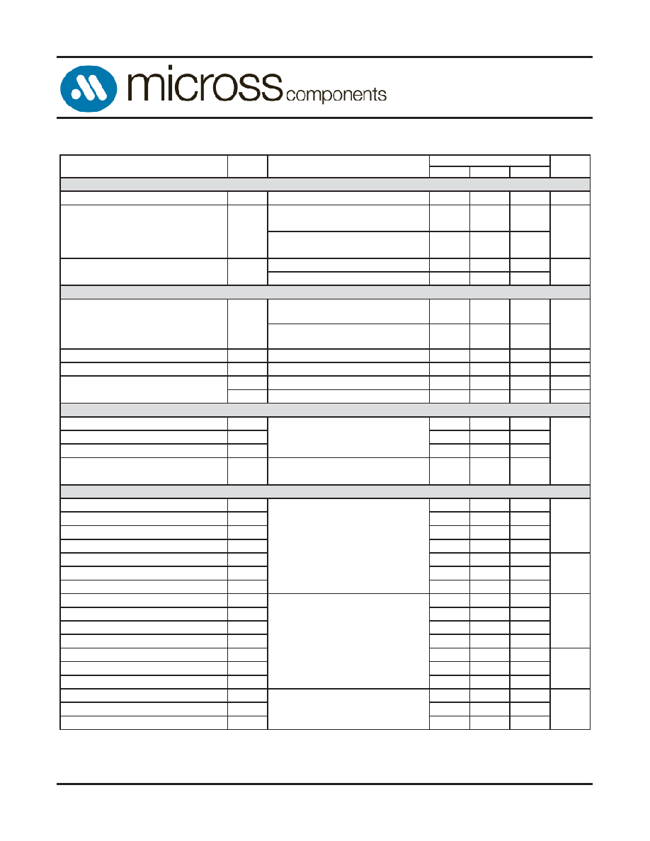
ADVANCED INFORMATION
Min
Typ
Max
Drain Source Blocking Voltage
BVDS
VGS = 15 V, ID = 600 A
1200
V
VDS = 1200 V, VGS = 15 V,
Tj = 25
oC
220
VDS = 1200 V, VGS = 15 V,
Tj = 150
oC
20
400
VGS = 15 V, VDS = 0V
0.1
0.6
VGS = 15 V, VDS = 1200V
0.1
ID = 40 A, VGS = 2 V,
Tj = 25 °C
0.035
0.045
ID = 40 A, VGS = 2 V,
Tj = 100 °C
0.07
Gate Threshold Voltage
VGS(th)
VDS = 1 V, ID = 34mA
6.00
4.00
V
Gate Forward Current
IGFWD
VGS = 2 V
0
mA
RG
f = 1 MHz, drain source shorted
4
RG(on)
VGS >2.7V
0.25
Input Capacitance
Ciss
1340
Output Capacitance
Coss
206
Reverse Transfer Capacitance
Crss
194
Effective Output Capacitance,
energy related
Co(er)
VDS = 0 V to 600 V,
VGS = 0 V
110
Turn On Delay
ton
TBD
Rise Time
tr
TBD
Turn Off Delay
toff
TBD
Fall Time
tf
TBD
Turn On Energy
Eon
TBD
Turn Off Energy
Eoff
TBD
Total Switching Energy
Ets
TBD
Turn On Delay
ton
TBD
Rise Time
tr
TBD
Turn Off Delay
toff
TBD
Fall Time
tf
TBD
Turn On Energy
Eon
TBD
Turn Off Energy
Eoff
TBD
Total Switching Energy
Ets
TBD
Total Gate Charge
Qg
65
Gate Source Charge
Qgs
4
Gate Drain Charge
Qgd
54
VDS = 600 V, ID = 40 A,
Inductive Load, TJ = 150
oC
VDS = 600V, ID = 5 A,
VGS = + 2.5 V
ns
μJ
ns
μJ
nC
Dynamic Characteristics
VDD = 100 V
pF
Switching Characteristics
VDS = 600 V, ID = 40 A,
Inductive Load, TJ = 25
oC
On Characteristics
Drain Source On resistance
Gate Resistance
RDS(on)
Total Gate Reverse Leakage
IGSS
μA
mA
Total Drain Leakage Current
IDSS
Off Characteristics
Value
Unit
Symbol
Parameter
Conditions
ELECTRICAL CHARACTERISTICS
發(fā)布緊急采購,3分鐘左右您將得到回復。