- 您現(xiàn)在的位置:買賣IC網(wǎng) > PDF目錄57938 > AO4800B (ALPHA AND OMEGA SEMICONDUCTOR) 6900 mA, 30 V, 2 CHANNEL, N-CHANNEL, Si, SMALL SIGNAL, MOSFET PDF資料下載
參數(shù)資料
| 型號(hào): | AO4800B |
| 廠商: | ALPHA AND OMEGA SEMICONDUCTOR |
| 元件分類: | 小信號(hào)晶體管 |
| 英文描述: | 6900 mA, 30 V, 2 CHANNEL, N-CHANNEL, Si, SMALL SIGNAL, MOSFET |
| 封裝: | GREEN, SOIC-8 |
| 文件頁(yè)數(shù): | 2/6頁(yè) |
| 文件大?。?/td> | 278K |
| 代理商: | AO4800B |
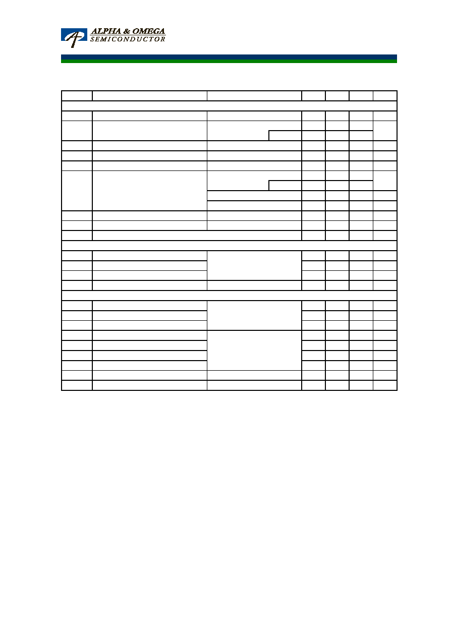
AO4800B
Symbol
Min
Typ
Max
Units
BVDSS
30
V
VDS=30V, VGS=0V
1
TJ=55°C
5
IGSS
100
nA
VGS(th)
Gate Threshold Voltage
0.7
1.1
1.5
V
ID(ON)
30
A
17.8
27
TJ=125°C
28
40
19
32
m
24
50
m
gFS
33
S
VSD
0.7
1
V
IS
2.5
A
Ciss
500
630
760
pF
Coss
50
75
100
pF
Crss
30
50
70
pF
Rg
1.5
3
4.5
Qg
4.8
6
7
nC
Qgs
1
1.3
1.6
nC
Qgd
1
1.8
2.5
nC
tD(on)
3
ns
tr
2.5
ns
tD(off)
25
ns
tf
4
ns
trr
7
8.5
10
ns
Qrr
2
2.6
3.1
nC
THIS PRODUCT HAS BEEN DESIGNED AND QUALIFIED FOR THE CONSUMER MARKET. APPLICATIONS OR USES AS CRITICAL
COMPONENTS IN LIFE SUPPORT DEVICES OR SYSTEMS ARE NOT AUTHORIZED. AOS DOES NOT ASSUME ANY LIABILITY ARISING
OUT OF SUCH APPLICATIONS OR USES OF ITS PRODUCTS. AOS RESERVES THE RIGHT TO IMPROVE PRODUCT DESIGN,
FUNCTIONS AND RELIABILITY WITHOUT NOTICE.
Body Diode Reverse Recovery Time
Drain-Source Breakdown Voltage
On state drain current
ID=250A, VGS=0V
VGS=4.5V, VDS=5V
VGS=10V, ID=6.9A
Reverse Transfer Capacitance
IF=6.9A, dI/dt=100A/s
VGS=0V, VDS=15V, f=1MHz
SWITCHING PARAMETERS
Forward Transconductance
Diode Forward Voltage
Electrical Characteristics (TJ=25°C unless otherwise noted)
STATIC PARAMETERS
Parameter
Conditions
IDSS
A
VDS=VGS ID=250A
VDS=0V, VGS= ±12V
Zero Gate Voltage Drain Current
Gate-Body leakage current
IS=1A,VGS=0V
VDS=5V, ID=5A
VGS=2.5V, ID=5A
VGS=4.5V, ID=6A
RDS(ON)
Static Drain-Source On-Resistance
m
Gate resistance
VGS=0V, VDS=0V, f=1MHz
Turn-Off Fall Time
Total Gate Charge
VGS=4.5V, VDS=15V, ID=6.9A
Gate Source Charge
Gate Drain Charge
Body Diode Reverse Recovery Charge IF=6.9A, dI/dt=100A/s
Maximum Body-Diode Continuous Current
Input Capacitance
Output Capacitance
Turn-On DelayTime
DYNAMIC PARAMETERS
Turn-On Rise Time
Turn-Off DelayTime
VGS=10V, VDS=15V, RL=2.2,
RGEN=3
A. The value of RθJA is measured with the device mounted on 1in
2 FR-4 board with 2oz. Copper, in a still air environment with T
A =25°C. The
value in any given application depends on the user's specific board design.
B. The power dissipation PD is based on TJ(MAX)=150°C, using ≤ 10s junction-to-ambient thermal resistance.
C. Repetitive rating, pulse width limited by junction temperature TJ(MAX)=150°C. Ratings are based on low frequency and duty cycles to keep
initialTJ=25°C.
D. The RθJA is the sum of the thermal impedence from junction to lead RθJL and lead to ambient.
E. The static characteristics in Figures 1 to 6 are obtained using <300
s pulses, duty cycle 0.5% max.
F. These curves are based on the junction-to-ambient thermal impedence which is measured with the device mounted on 1in
2 FR-4 board with
2oz. Copper, assuming a maximum junction temperature of TJ(MAX)=150°C. The SOA curve provides a single pulse ratin g.
Rev 3: Oct 2010
www.aosmd.com
Page 2 of 6
相關(guān)PDF資料 |
PDF描述 |
|---|---|
| AO4812 | 6000 mA, 30 V, 2 CHANNEL, N-CHANNEL, Si, SMALL SIGNAL, MOSFET |
| AO4813 | 7100 mA, 30 V, 2 CHANNEL, P-CHANNEL, Si, SMALL SIGNAL, MOSFET |
| AO4822 | 8000 mA, 30 V, 2 CHANNEL, N-CHANNEL, Si, SMALL SIGNAL, MOSFET |
| AO4932 | 8000 mA, 30 V, 2 CHANNEL, N-CHANNEL, Si, SMALL SIGNAL, MOSFET |
| AO6402A | 30 V, 0.027 ohm, N-CHANNEL, Si, POWER, MOSFET |
相關(guān)代理商/技術(shù)參數(shù) |
參數(shù)描述 |
|---|---|
| AO4800B_11 | 制造商:AOSMD 制造商全稱:Alpha & Omega Semiconductors 功能描述:30V Dual N-Channel MOSFET |
| AO4800BL | 制造商:AOS 功能描述:MOSFET |
| AO4800C | 制造商:AOSMD 制造商全稱:Alpha & Omega Semiconductors 功能描述:30V Dual N-Channel MOSFET |
| AO4800L | 制造商:AOSMD 制造商全稱:Alpha & Omega Semiconductors 功能描述:Plastic Encapsulated Device |
| AO4801 | 制造商:AOS 功能描述:MOSFET |
發(fā)布緊急采購(gòu),3分鐘左右您將得到回復(fù)。