參數資料
| 型號: | AMIS42673ICAG1G |
| 廠商: | ON Semiconductor |
| 文件頁數: | 9/11頁 |
| 文件大小: | 0K |
| 描述: | IC TXRX CAN DGTL 3.3V HS 8SOIC |
| 標準包裝: | 96 |
| 類型: | 收發(fā)器 |
| 驅動器/接收器數: | 1/1 |
| 規(guī)程: | CAN |
| 電源電壓: | 4.75 V ~ 5.25 V |
| 安裝類型: | 表面貼裝 |
| 封裝/外殼: | 8-SOIC(0.154",3.90mm 寬) |
| 供應商設備封裝: | 8-SOICN |
| 包裝: | 管件 |
AMIS42673
http://onsemi.com
7
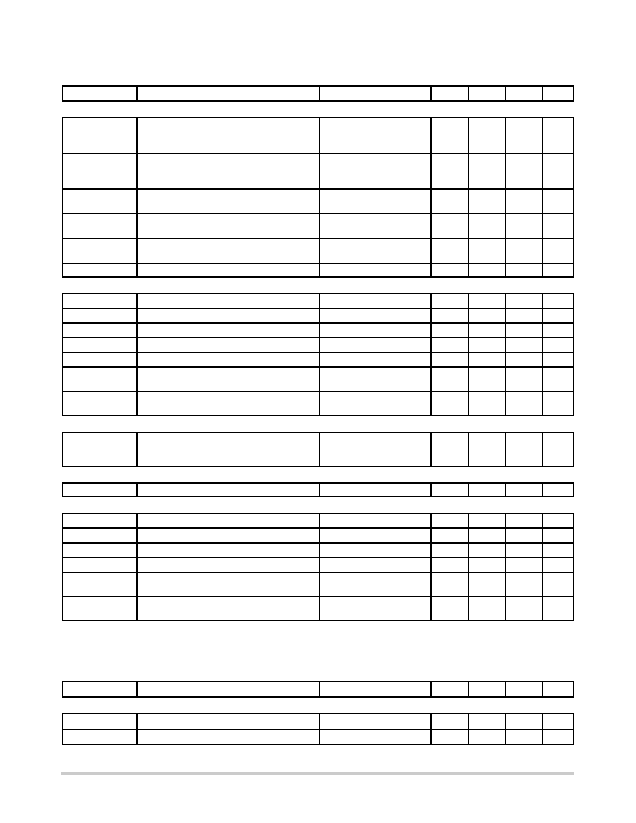
Table 6. DC CHARACTERISTICS VCC = 4.75 V to 5.25 V, V33 = 2.9 V to 3.6 V; TJ = 40°C to +150°C; RLT = 60 W unless specified
otherwise.
Symbol
Unit
Max
Typ
Min
Conditions
Parameter
BUS LINES (Pins CANH and CANL)
Vihcm(dif)(th)
Differential Receiver Threshold Voltage for
High CommonMode
35 V <
VCANL < +35 V;
35 V <
VCANH < +35 V;
See Figure 4
0.25
0.7
1.05
V
Vi(dif)(hys)
Differential Receiver Input Voltage Hysteresis
35 V <
VCANL < +35 V;
35 V <
VCANH < +35 V;
See Figure 4
50
70
100
mV
Ri(cm)(CANH)
CommonMode Input Resistance at Pin
CANH
15
25
37
kW
Ri(cm) (CANL)
CommonMode Input Resistance at Pin
CANL
15
25
37
kW
Ri(cm)(m)
Matching Between Pin CANH and Pin CANL
CommonMode Input Resistance
VCANH = VCANL
3
0
+3
%
Ri(dif)
Differential Input Resistance
25
50
75
kW
BUS LINES (Pins CANH and CANL)
Ci(CANH)
Input Capacitance at Pin CANH
VTxD = VCC; Not Tested
7.5
20
pF
Ci(CANL)
Input Capacitance at Pin CANL
VTxD = VCC; Not Tested
7.5
20
pF
Ci(dif)
Differential Input Capacitance
VTxD = VCC; Not Tested
3.75
10
pF
ILI(CANH)
Input Leakage Current at Pin CANH
VCC = 0 V; VCANH = 5 V
10
170
250
mA
ILI(CANL)
Input Leakage Current at Pin CANL
VCC = 0 V; VCANL = 5 V
10
170
250
mA
VCMpeak
CommonMode Peak During Transition from
Dom → Rec or Rec → Dom
500
mV
VCMstep
Difference in CommonMode Between
Dominant and Recessive State
150
mV
POWERONRESET
PORL
POR Level
CANH, CANL,
Vref in
TriState Below POR
Level
2.2
3.5
4.7
V
THERMAL SHUTDOWN
TJ(sd)
Shutdown Junction Temperature
150
160
180
°C
TIMING CHARACTERISTICS (See Figures 6 and 7)
td(TxDBUSon)
Delay TxD to Bus Active
40
85
110
ns
td(TxDBUSoff)
Delay TxD to Bus Inactive
30
60
110
ns
td(BUSonRxD)
Delay Bus Active to RxD
25
55
110
ns
td(BUSoffRxD)
Delay Bus Inactive to RxD
65
100
135
ns
tpd(recdom)
Propagation Delay TxD to RxD from
Recessive to Dominant
100
230
ns
td(domrec)
Propagation Delay TxD to RxD from
Dominant to Recessive
100
245
ns
7. Not tested at ATE
Table 7. DIGITAL OUTPUT CHARACTERISTICS @ V33 = 2.5 V VCC = 4.75 to 5.25 V; V33 = 2.5 V $5%; TJ = 40 to +150°C;
RLT = 60 W unless specified otherwise.
Symbol
Parameter
Conditions
Min
Typ
Max
Unit
RECEIVER DATA OUTPUT (Pin RxD)
Ioh
HIGHLevel Output Current
VOH > 0.9 x V33
2.6
mA
Iol
LOWLevel Output Current
VOL < 0.1 x V33
4
mA
相關PDF資料 |
PDF描述 |
|---|---|
| AMIS42675ICAA1G | IC TRANSCEIVER CAN LP HS 8SOIC |
| AMIS42700WCGA4RH | IC TXRX CAN DUAL HS 20SOIC |
| AMIS42770ICAW1G | IC TXRX CAN DUAL HS 20SOIC |
| AMIS49587C5872G | IC MODEM PLC 50/60MHZ 52QFN |
| AOZ6184QT | IC USB 2.0 SWITCH DPDT 10QFN |
相關代理商/技術參數 |
參數描述 |
|---|---|
| AMIS42673ICAG1RG | 功能描述:CAN 接口集成電路 HS CAN TRANSCEIVER RoHS:否 制造商:Texas Instruments 類型:Transceivers 工作電源電壓:5 V 電源電流: 工作溫度范圍:- 40 C to + 85 C 封裝 / 箱體:SOIC-8 封裝:Tube |
| AMIS-42675 | 制造商:ONSEMI 制造商全稱:ON Semiconductor 功能描述:High Speed Low Power CAN Transceiver for Long Wire Networks |
| AMIS-42675AGA | 制造商:AMI 制造商全稱:AMI 功能描述:High-Speed Low Power CAN Transceiver |
| AMIS42675ICAA1G | 功能描述:CAN 接口集成電路 HS LOW POWER TRANSCEIVER RoHS:否 制造商:Texas Instruments 類型:Transceivers 工作電源電壓:5 V 電源電流: 工作溫度范圍:- 40 C to + 85 C 封裝 / 箱體:SOIC-8 封裝:Tube |
| AMIS42675ICAA1RG | 功能描述:CAN 接口集成電路 HS LOW POWER TRANSCEIVER RoHS:否 制造商:Texas Instruments 類型:Transceivers 工作電源電壓:5 V 電源電流: 工作溫度范圍:- 40 C to + 85 C 封裝 / 箱體:SOIC-8 封裝:Tube |
發(fā)布緊急采購,3分鐘左右您將得到回復。