- 您現(xiàn)在的位置:買賣IC網(wǎng) > PDF目錄375310 > AM70PDL127CDH85IT (SPANSION LLC) Stacked Multi-Chip Package (MCP/XIP) Flash Memory, Data storage MirrorBit Flash, and pSRAM (XIP) PDF資料下載
參數(shù)資料
| 型號(hào): | AM70PDL127CDH85IT |
| 廠商: | SPANSION LLC |
| 元件分類: | 存儲(chǔ)器 |
| 英文描述: | Stacked Multi-Chip Package (MCP/XIP) Flash Memory, Data storage MirrorBit Flash, and pSRAM (XIP) |
| 中文描述: | SPECIALTY MEMORY CIRCUIT, PBGA93 |
| 封裝: | 13 X 9 MM, FBGA-93 |
| 文件頁(yè)數(shù): | 107/127頁(yè) |
| 文件大小: | 846K |
| 代理商: | AM70PDL127CDH85IT |
第1頁(yè)第2頁(yè)第3頁(yè)第4頁(yè)第5頁(yè)第6頁(yè)第7頁(yè)第8頁(yè)第9頁(yè)第10頁(yè)第11頁(yè)第12頁(yè)第13頁(yè)第14頁(yè)第15頁(yè)第16頁(yè)第17頁(yè)第18頁(yè)第19頁(yè)第20頁(yè)第21頁(yè)第22頁(yè)第23頁(yè)第24頁(yè)第25頁(yè)第26頁(yè)第27頁(yè)第28頁(yè)第29頁(yè)第30頁(yè)第31頁(yè)第32頁(yè)第33頁(yè)第34頁(yè)第35頁(yè)第36頁(yè)第37頁(yè)第38頁(yè)第39頁(yè)第40頁(yè)第41頁(yè)第42頁(yè)第43頁(yè)第44頁(yè)第45頁(yè)第46頁(yè)第47頁(yè)第48頁(yè)第49頁(yè)第50頁(yè)第51頁(yè)第52頁(yè)第53頁(yè)第54頁(yè)第55頁(yè)第56頁(yè)第57頁(yè)第58頁(yè)第59頁(yè)第60頁(yè)第61頁(yè)第62頁(yè)第63頁(yè)第64頁(yè)第65頁(yè)第66頁(yè)第67頁(yè)第68頁(yè)第69頁(yè)第70頁(yè)第71頁(yè)第72頁(yè)第73頁(yè)第74頁(yè)第75頁(yè)第76頁(yè)第77頁(yè)第78頁(yè)第79頁(yè)第80頁(yè)第81頁(yè)第82頁(yè)第83頁(yè)第84頁(yè)第85頁(yè)第86頁(yè)第87頁(yè)第88頁(yè)第89頁(yè)第90頁(yè)第91頁(yè)第92頁(yè)第93頁(yè)第94頁(yè)第95頁(yè)第96頁(yè)第97頁(yè)第98頁(yè)第99頁(yè)第100頁(yè)第101頁(yè)第102頁(yè)第103頁(yè)第104頁(yè)第105頁(yè)第106頁(yè)當(dāng)前第107頁(yè)第108頁(yè)第109頁(yè)第110頁(yè)第111頁(yè)第112頁(yè)第113頁(yè)第114頁(yè)第115頁(yè)第116頁(yè)第117頁(yè)第118頁(yè)第119頁(yè)第120頁(yè)第121頁(yè)第122頁(yè)第123頁(yè)第124頁(yè)第125頁(yè)第126頁(yè)第127頁(yè)
November 24, 2003
Am70PDL127CDH/Am70PDL129CDH
105
A D V A N C E I N F O R M A T I O N
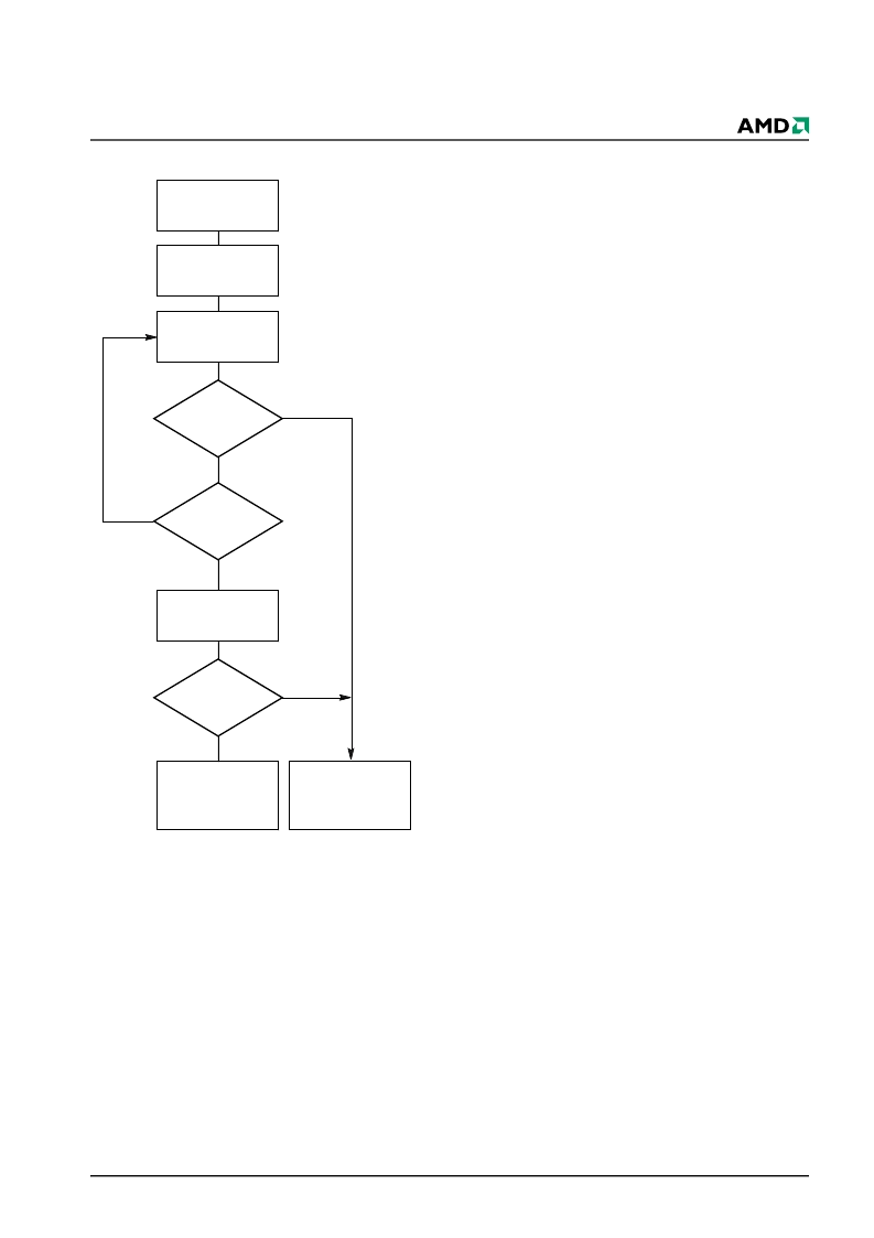
Figure 9.
Toggle Bit Algorithm
DQ2: Toggle Bit II
The “Toggle Bit II” on DQ2, when used with DQ6, indi-
cates whether a particular sector is actively erasing
(that is, the Embedded Erase algorithm is in progress),
or whether that sector is erase-suspended. Toggle Bit
II is valid after the rising edge of the final WE# pulse in
the command sequence.
DQ2 toggles when the system reads at addresses
within those sectors that have been selected for era-
sure. (The system may use either OE# or CE# to con-
trol the read cycles.) But DQ2 cannot distinguish
whether the sector is actively erasing or is erase-sus-
pended. DQ6, by comparison, indicates whether the
device is actively erasing, or is in Erase Suspend, but
cannot distinguish which sectors are selected for era-
sure. Thus, both status bits are required for sector and
mode information. Refer to
Table 12
to compare out-
puts for DQ2 and DQ6.
Figure 9 shows the toggle bit algorithm in flowchart
form, and the section “DQ2: Toggle Bit II” explains the
algorithm. See also the
RY/BY#: Ready/Busy#
sub-
section. Figure 21 shows the toggle bit timing diagram.
Figure 22 shows the differences between DQ2 and
DQ6 in graphical form.
Reading Toggle Bits DQ6/DQ2
Refer to Figure 9 for the following discussion. When-
ever the system initially begins reading toggle bit sta-
tus, it must read DQ7–DQ0 at least twice in a row to
determine whether a toggle bit is toggling. Typically,
the system would note and store the value of the tog-
gle bit after the first read. After the second read, the
system would compare the new value of the toggle bit
with the first. If the toggle bit is not toggling, the device
has completed the program or erase operation. The
system can read array data on DQ7–DQ0 on the fol-
lowing read cycle.
However, if after the initial two read cycles, the system
determines that the toggle bit is still toggling, the sys-
tem also should note whether the value of DQ5 is high
(see the section on DQ5). If it is, the system should
then determine again whether the toggle bit is tog-
gling, since the toggle bit may have stopped toggling
just as DQ5 went high. If the toggle bit is no longer
toggling, the device has successfully completed the
program or erase operation. If it is still toggling, the de-
vice did not completed the operation successfully, and
the system must write the reset command to return to
reading array data.
The remaining scenario is that the system initially de-
termines that the toggle bit is toggling and DQ5 has
not gone high. The system may continue to monitor
the toggle bit and DQ5 through successive read cy-
cles, determining the status as described in the previ-
ous paragraph. Alternatively, it may choose to perform
START
No
Yes
Yes
DQ5 = 1
No
Yes
Toggle Bit
= Toggle
No
Program/Erase
Operation Not
Complete, Write
Reset Command
Program/Erase
Operation Complete
Toggle Bit
= Toggle
Read Byte Twice
(DQ7–DQ0)
Address = VA
Read Byte
(DQ7–DQ0)
Address =VA
Read Byte
(DQ7–DQ0)
Address =VA
Note:
The system should recheck the toggle bit even if
DQ5 = “1” because the toggle bit may stop toggling as DQ5
changes to “1.” See the subsections on DQ6 and DQ2 for
more information.
相關(guān)PDF資料 |
PDF描述 |
|---|---|
| AM70PDL129CDH | Stacked Multi-Chip Package (MCP/XIP) Flash Memory, Data storage MirrorBit Flash, and pSRAM (XIP) |
| AM70PDL129CDH66I | Stacked Multi-Chip Package (MCP/XIP) Flash Memory, Data storage MirrorBit Flash, and pSRAM (XIP) |
| AM70PDL129CDH66IS | Stacked Multi-Chip Package (MCP/XIP) Flash Memory, Data storage MirrorBit Flash, and pSRAM (XIP) |
| AM70PDL129CDH66IT | Stacked Multi-Chip Package (MCP/XIP) Flash Memory, Data storage MirrorBit Flash, and pSRAM (XIP) |
| AM70PDL129CDH85I | Stacked Multi-Chip Package (MCP/XIP) Flash Memory, Data storage MirrorBit Flash, and pSRAM (XIP) |
相關(guān)代理商/技術(shù)參數(shù) |
參數(shù)描述 |
|---|---|
| AM70PDL129BDH | 制造商:SPANSION 制造商全稱:SPANSION 功能描述:2 x 64 Megabit (8 M x 16-Bit) CMOS 3.0 Volt-Only Page Mode Flash Memory Data Storage 128 Megabit (8 M x 16-Bit) CMOS |
| AM70PDL129BDH66I | 制造商:SPANSION 制造商全稱:SPANSION 功能描述:Stacked Multi-Chip Package (MCP/XIP) Flash Memory, Data storage MirrorBit Flash, and pSRAM (XIP) |
| AM70PDL129BDH66IS | 制造商:SPANSION 制造商全稱:SPANSION 功能描述:2 x 64 Megabit (8 M x 16-Bit) CMOS 3.0 Volt-Only Page Mode Flash Memory Data Storage 128 Megabit (8 M x 16-Bit) CMOS |
| AM70PDL129BDH66IT | 制造商:SPANSION 制造商全稱:SPANSION 功能描述:2 x 64 Megabit (8 M x 16-Bit) CMOS 3.0 Volt-Only Page Mode Flash Memory Data Storage 128 Megabit (8 M x 16-Bit) CMOS |
| AM70PDL129BDH85I | 制造商:SPANSION 制造商全稱:SPANSION 功能描述:Stacked Multi-Chip Package (MCP/XIP) Flash Memory, Data storage MirrorBit Flash, and pSRAM (XIP) |
發(fā)布緊急采購(gòu),3分鐘左右您將得到回復(fù)。