- 您現(xiàn)在的位置:買賣IC網(wǎng) > PDF目錄375309 > AM6012 (NXP Semiconductors N.V.) 12-Bit multiplying D/A converter PDF資料下載
參數(shù)資料
| 型號: | AM6012 |
| 廠商: | NXP Semiconductors N.V. |
| 英文描述: | 12-Bit multiplying D/A converter |
| 中文描述: | 12位乘法D / A轉(zhuǎn)換器 |
| 文件頁數(shù): | 9/11頁 |
| 文件大小: | 107K |
| 代理商: | AM6012 |
Philips Semiconductors Linear Products
Product specification
AM6012
12-Bit multiplying D/A converter
August 31, 1994
784
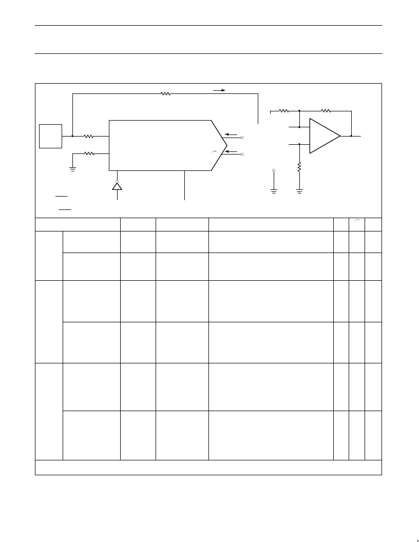
APPLICATION CIRCUITS
Figure 4. AM6012 Logic Inputs
CODE FORMAT
CONNECTIONS
OUTPUT SCALE
MSB
B1
LSB
B12
B2
B3
B4
B5
B6
B7
B8
B9
B10 B11
I
(mA)
I
(mA)
V
OUT
Unipolar
Symmetrical
Offset
Offset with
True Zero
Straight binary; one
polarity with true input
code, true zero output.
Complementary binary;
one polarity with
complementary input
code, true zero output.
Straight offset binary;
offset half-scale,
symmetrical about zero,
no true zero output.
1’s complement; offset
half-scale, symmetrical
about zero, no true zero
output, MSB complemented
(need inverter at B1).
Offset binary; offset half-
scale, true zero output.
2’s complement; offset
half-scale, true zero
output, MSB complemented
(need inverter at B1).
a – c
b – g
R1 = R2 = 2.5k
a – g
b – c
R1 = R2 = 2.5k
a – c
b – d
f – g
R1 = R3 = 2.5k
R2 = 1.25k
a – c
b – d
f – g
R1 = R3 = 2.5k
R2 = 1.25k
e – a – c
b – g
R1 = R2 = 5k
e – a – c
b – g
R1 = R2 = 5k
Positive full-scale
Positive full-scale – LSB
Zero-scale
Positive full-scale
Positive full-scale – LSB
Zero-scale
Positive full-scale
Positive full-scale – LSB
(+) Zero-scale
(–) Zero-scale
Negative full-scale – LSB
Negative full-scale
Positive full-scale
Positive full-scale – LSB
(+) Zero-scale
(–) Zero-scale
Negative full-scale – LSB
Negative full-scale
Positive full-scale
Positive full-scale – LSB
+ LSB
Zero-scale
– LSB
Negative full-scale + LSB
Negative full-scale
R14
VREF
1.0mA
VREF
2.0mA
ROFF
Positive full-scale
Positive full-scale – LSB
+ 1 LSB
Zero-scale
– 1 LSB
Negative full-scale + LSB
Negative full-scale
1
1
0
1
1
0
1
1
0
1
1
0
1
1
0
1
1
0
1
1
0
1
1
0
1
1
0
1
1
0
1
1
0
1
0
0
3.999
3.998
0.000
0.000
0.001
3.999
9.9976
9.9951
0.0000
0
0
1
0
0
1
0
0
1
0
0
1
0
0
1
0
0
1
0
0
1
0
0
1
0
0
1
0
0
1
0
0
1
0
1
1
0.000
0.001
3.999
3.999
3.998
0.000
9.9976
9.9951
0.0000
1
1
1
0
0
0
1
1
0
1
0
0
1
1
0
1
0
0
1
1
0
1
0
0
1
1
0
1
0
0
1
1
0
1
0
0
1
1
0
1
0
0
1
1
0
1
0
0
1
1
0
1
0
0
1
1
0
1
0
0
1
1
0
1
0
0
1
0
0
1
1
0
3.999
3.998
2.000
1.999
0.001
0.000
0.000
0.001
1.999
2.000
3.998
3.999
9.9976
9.9927
0.0024
–0.0024
–9.9927
–9.9976
0
0
0
1
1
1
1
1
0
1
0
0
1
1
0
1
0
0
1
1
0
1
0
0
1
1
0
1
0
0
1
1
0
1
0
0
1
1
0
1
0
0
1
1
0
1
0
0
1
1
0
1
0
0
1
1
0
1
0
0
1
1
0
1
0
0
1
0
0
1
1
0
3.999
3.998
2.000
1.999
0.001
0.000
0.000
0.001
1.999
2.000
3.998
3.999
9.9976
9.9927
0.0024
–0.0024
–9.9927
–9.9976
1
1
1
1
0
0
0
1
1
0
0
1
0
0
1
1
0
0
1
0
0
1
1
0
0
1
0
0
1
1
0
0
1
0
0
1
1
0
0
1
0
0
1
1
0
0
1
0
0
1
1
0
0
1
0
0
1
1
0
0
1
0
0
1
1
0
0
1
0
0
1
1
0
0
1
0
0
1
0
1
0
1
1
0
3.999
3.998
2.001
2.000
1.999
0.001
0.000
0.000
0.001
1.998
1.999
2.000
3.998
3.999
9.9951
9.9902
0.0049
0.000
–0.0049
–9.9951
–10.000
0
0
0
0
1
1
1
1
1
0
0
1
0
0
1
1
0
0
1
0
0
1
1
0
0
1
0
0
1
1
0
0
1
0
0
1
1
0
0
1
0
0
1
1
0
0
1
0
0
1
1
0
0
1
0
0
1
1
0
0
1
0
0
1
1
0
0
1
0
0
1
1
0
0
1
0
0
1
0
1
0
1
1
0
3.998
2.001
2.000
1.999
0.001
0.000
0.001
1.998
1.999
2.000
3.998
3.999
9.9902
0.0049
0.000
–0.049
–9.9951
–10.000
AM6012
V
REF(+)
V
REF(–)
+10V
REF
OPTIONAL
(SEE CODE TABLE)
MSB
LSB
R
OFF
5,000k
2.000mA
a
b
B
12
B
1
I
O
I
O
e
V
OUT
R
1
R
3
R
14
10k
R
15
10k
f
R
2
c
d
g
NE535
–
+
ADDITIONAL CODE MODIFICATIONS
1. Any of the offset binary codes may be complemented by
reversing the output terminal pair.
相關(guān)PDF資料 |
PDF描述 |
|---|---|
| AM6012D | 12-Bit multiplying D/A converter |
| AM6012F | Circular Connector; No. of Contacts:6; Series:MS27505; Body Material:Aluminum; Connecting Termination:Crimp; Connector Shell Size:9; Circular Contact Gender:Socket; Circular Shell Style:Box Mount Receptacle; Insert Arrangement:9-35 RoHS Compliant: No |
| AM6651B | MOTOR CONTROL CIRCUIT |
| AM6651BU | MOTOR CONTROL CIRCUIT |
| AM6651BU-E1 | MOTOR CONTROL CIRCUIT |
相關(guān)代理商/技術(shù)參數(shù) |
參數(shù)描述 |
|---|---|
| AM6012/BRA | 制造商:未知廠家 制造商全稱:未知廠家 功能描述:12-Bit Digital-to-Analog Converter |
| AM6012A | 制造商:未知廠家 制造商全稱:未知廠家 功能描述: |
| AM6012ACWP | 制造商:未知廠家 制造商全稱:未知廠家 功能描述:12-Bit Digital-to-Analog Converter |
| AM6012AD | 制造商:未知廠家 制造商全稱:未知廠家 功能描述:12-Bit Digital-to-Analog Converter |
| AM6012ADC | 制造商:未知廠家 制造商全稱:未知廠家 功能描述:12-Bit Digital-to-Analog Converter |
發(fā)布緊急采購,3分鐘左右您將得到回復(fù)。