- 您現(xiàn)在的位置:買(mǎi)賣(mài)IC網(wǎng) > PDF目錄366487 > AM29LV160DB-90FC (Advanced Micro Devices, Inc.) 16 Megabit (2 M x 8-Bit/1 M x 16-Bit) CMOS 3.0 Volt-only Boot Sector Flash Memory PDF資料下載
參數(shù)資料
| 型號(hào): | AM29LV160DB-90FC |
| 廠商: | Advanced Micro Devices, Inc. |
| 元件分類(lèi): | FLASH |
| 英文描述: | 16 Megabit (2 M x 8-Bit/1 M x 16-Bit) CMOS 3.0 Volt-only Boot Sector Flash Memory |
| 中文描述: | 16Mb(2M×8位/1Mx16位), 3V, CMOS引導(dǎo)扇區(qū)閃存 |
| 文件頁(yè)數(shù): | 9/52頁(yè) |
| 文件大?。?/td> | 844K |
| 代理商: | AM29LV160DB-90FC |
第1頁(yè)第2頁(yè)第3頁(yè)第4頁(yè)第5頁(yè)第6頁(yè)第7頁(yè)第8頁(yè)當(dāng)前第9頁(yè)第10頁(yè)第11頁(yè)第12頁(yè)第13頁(yè)第14頁(yè)第15頁(yè)第16頁(yè)第17頁(yè)第18頁(yè)第19頁(yè)第20頁(yè)第21頁(yè)第22頁(yè)第23頁(yè)第24頁(yè)第25頁(yè)第26頁(yè)第27頁(yè)第28頁(yè)第29頁(yè)第30頁(yè)第31頁(yè)第32頁(yè)第33頁(yè)第34頁(yè)第35頁(yè)第36頁(yè)第37頁(yè)第38頁(yè)第39頁(yè)第40頁(yè)第41頁(yè)第42頁(yè)第43頁(yè)第44頁(yè)第45頁(yè)第46頁(yè)第47頁(yè)第48頁(yè)第49頁(yè)第50頁(yè)第51頁(yè)第52頁(yè)
22358B7
May 5, 2006
Am29LV160D
7
D A T A S H E E T
PIN CONFIGURATION
A0–A19
=20 addresses
DQ0–DQ14 =15 data inputs/outputs
DQ15/A-1
=DQ15 (data input/output, word mode),
A-1 (LSB address input, byte mode)
BYTE#
=Selects 8-bit or 16-bit mode
CE#
=Chip enable
OE#
= Output enable
WE#
=Write enable
RESET#
=Hardware reset pin
RY/BY#
= Ready/Busy output
(N/A SO 044)
V
CC
=3.0 volt-only single power supply
(see Product Selector Guide for speed
options and voltage supply tolerances)
V
SS
NC
=Device ground
=Pin not connected internally
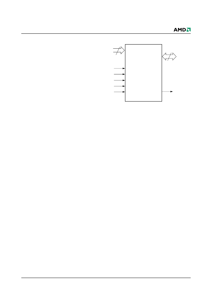
LOGIC SYMBOL
20
16 or 8
DQ0–DQ15
(A-1)
A0–A19
CE#
OE#
WE#
RESET#
BYTE#
RY/BY#
(N/A SO 044)
發(fā)布緊急采購(gòu),3分鐘左右您將得到回復(fù)。