- 您現(xiàn)在的位置:買賣IC網(wǎng) > PDF目錄375289 > AM29BDS320GBC9VMI (SPANSION LLC) 32 Megabit (2 M x 16-Bit), 1.8 Volt-only Simultaneous Read/Write, Burst Mode Flash Memory PDF資料下載
參數(shù)資料
| 型號: | AM29BDS320GBC9VMI |
| 廠商: | SPANSION LLC |
| 元件分類: | DRAM |
| 英文描述: | 32 Megabit (2 M x 16-Bit), 1.8 Volt-only Simultaneous Read/Write, Burst Mode Flash Memory |
| 中文描述: | 2M X 16 FLASH 1.8V PROM, 90 ns, PBGA64 |
| 封裝: | 8 X 9 MM, 0.80 MM PITCH, FBGA-64 |
| 文件頁數(shù): | 31/74頁 |
| 文件大?。?/td> | 701K |
| 代理商: | AM29BDS320GBC9VMI |
第1頁第2頁第3頁第4頁第5頁第6頁第7頁第8頁第9頁第10頁第11頁第12頁第13頁第14頁第15頁第16頁第17頁第18頁第19頁第20頁第21頁第22頁第23頁第24頁第25頁第26頁第27頁第28頁第29頁第30頁當前第31頁第32頁第33頁第34頁第35頁第36頁第37頁第38頁第39頁第40頁第41頁第42頁第43頁第44頁第45頁第46頁第47頁第48頁第49頁第50頁第51頁第52頁第53頁第54頁第55頁第56頁第57頁第58頁第59頁第60頁第61頁第62頁第63頁第64頁第65頁第66頁第67頁第68頁第69頁第70頁第71頁第72頁第73頁第74頁
October 1, 2003 27243B1
Am29BDS320G
29
P r e l i m i n a r y
edge is active for all synchronous accesses. Address bit A17 determines this set-
ting; “1” for rising active, “0” for falling active.
RDY Configuration
By default, the device is set so that the RDY pin will output V
OH
whenever there
is valid data on the outputs. The device can be set so that RDY goes active one
data cycle before active data. Address bit A18 determines this setting; “1” for
RDY active with data, “0” for RDY active one clock cycle before valid data.
Configuration Register
Table 12
shows the address bits that determine the configuration register settings
for various device functions.
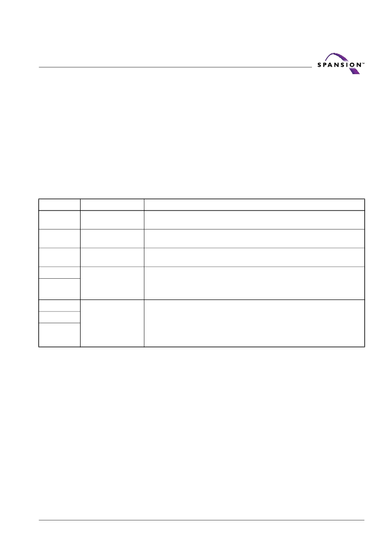
Table 12. Burst Mode Configuration Register
Note:
Device will be in the default state upon power-up or hardware reset.
Sector Lock/Unlock Command Sequence
The sector lock/unlock command sequence allows the system to determine which
sectors are protected from accidental writes. When the device is first powered up,
all sectors are locked. To unlock a sector, the system must write the sector lock/
unlock command sequence. In the first and second cycles, the address must point
to the bank that contains the sector(s) to be locked or unlocked. The first and
second cycle data is 60h. In the third cycle, the address must point to the target
sector, and A6 is used to specify a lock (A6 = V
IL
) or unlock (A6 = V
IH
) operation.
The third cycle data is 60h. After the third cycle, the system can continue to lock
or unlock additional sectors in the same bank or exit the sector lock/unlock se-
quence by writing the reset command (F0h).
It is not possible to read from the bank selected for sector lock/unlock operations.
To enable such read operations, write the reset command.
Note that the last two outermost boot sectors can be locked by taking the WP#
signal to V
IL
.
Address Bit
Function
Settings ( Binary)
A19
Set Device Read Mode
0 = Synchronous Read (Burst Mode) Enabled
1 = Asynchronous Mode (default)
A18
RDY
0 = RDY active one clock cycle before data
1 = RDY active with data (default)
A17
Clock
0 = Burst starts and data is output on the falling edge of CLK
1 = Burst starts and data is output on the rising edge of CLK (default)
A16
Burst Read Mode
00 = Continuous (default)
01 = 8-word linear with wrap around
10 = 16-word linear with wrap around
11 = 32-word linear with wrap around
A15
A14
Programmable
Wait State
000 = Data is valid on the 2nd active CLK edge after AVD# transition to V
IH
001 = Data is valid on the 3rd active CLK edge after AVD# transition to V
IH
010 = Data is valid on the 4th active CLK edge after AVD# transition to V
IH
011 = Data is valid on the 5th active CLK edge after AVD# transition to V
IH
100 = Data is valid on the 6th active CLK edge after AVD# transition to V
IH
101 = Data is valid on the 7th active CLK edge after AVD# transition to V
IH
(default)
A13
A12
相關PDF資料 |
PDF描述 |
|---|---|
| AM29BDS320GBD3VMI | 32 Megabit (2 M x 16-Bit), 1.8 Volt-only Simultaneous Read/Write, Burst Mode Flash Memory |
| AM29BDS320GBD4VMI | 32 Megabit (2 M x 16-Bit), 1.8 Volt-only Simultaneous Read/Write, Burst Mode Flash Memory |
| AM29BDS320GBD8VMI | 32 Megabit (2 M x 16-Bit), 1.8 Volt-only Simultaneous Read/Write, Burst Mode Flash Memory |
| AM29BDS320GBD9VMI | 32 Megabit (2 M x 16-Bit), 1.8 Volt-only Simultaneous Read/Write, Burst Mode Flash Memory |
| AM29BDS320GTC4VMI | 32 Megabit (2 M x 16-Bit), 1.8 Volt-only Simultaneous Read/Write, Burst Mode Flash Memory |
相關代理商/技術參數(shù) |
參數(shù)描述 |
|---|---|
| AM29BDS643GT5KVAI | 制造商:Spansion 功能描述:FLASH PARALLEL 1.8V 64MBIT 4MX16 55NS 44FBGA - Trays |
| AM29BL802CB-65RZET | 制造商:Spansion 功能描述: |
| AM29C01WW WAF | 制造商:Advanced Micro Devices 功能描述: |
| AM29C10API | 制造商:Rochester Electronics LLC 功能描述:- Bulk |
| AM29C10AWW DIE | 制造商:Advanced Micro Devices 功能描述: |
發(fā)布緊急采購,3分鐘左右您將得到回復。