- 您現(xiàn)在的位置:買賣IC網(wǎng) > PDF目錄92913 > AH118-89G 60 MHz - 3500 MHz RF/MICROWAVE WIDE BAND MEDIUM POWER AMPLIFIER PDF資料下載
參數(shù)資料
| 型號: | AH118-89G |
| 元件分類: | 放大器 |
| 英文描述: | 60 MHz - 3500 MHz RF/MICROWAVE WIDE BAND MEDIUM POWER AMPLIFIER |
| 封裝: | GREEN, TO-243C, SOT-89, 3 PIN |
| 文件頁數(shù): | 7/8頁 |
| 文件大小: | 266K |
| 代理商: | AH118-89G |
Specifications and information are subject to change without notice
WJ Communications, Inc
Phone 1-800-WJ1-4401 FAX: 408-577-6621 e-mail: sales@wj.com Web site: www.wj.com, www.TriQuint.com
Page 7 of 8 January 2008
AH118
Watt, High Linearity InGaP HBT Amplifier
450 MHz Reference Design
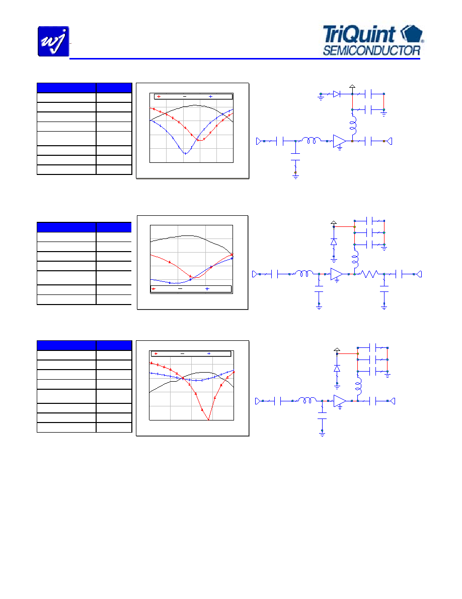
Frequency
450 MHz
Gain
22 dB
Input Return Loss
15 dB
Output Return Loss
19 dB
Output P1dB
+24 dBm
Output IP3
(+11 dBm / tone,
Df=1 MHz)
+40 dBm
Noise Figure
5.7 dB
Supply Voltage
+5 V
Current
160 mA
400
420
440
460
480
500
Frequency (MHz)
Gain / Return Loss
18
19
20
21
22
23
Ga
in
(
d
B
)
-25
-20
-15
-10
-5
0
S
11,
S
22
(
d
B
)
DB(|S(1,1)|) (R)
DB(|S(2,1)|) (L)
DB(|S(2,2)|) (R)
C=1000 pF
C=1e5 pF
L=22 nH
C=27 pF
L=3.3 nH
NET="AH118"
5.6 V
The diode D1 is used as over-voltage protection on the evaluation
boards. It is not specifically required in the final circuit layout in
a system using a DC regulator.
Vcc = +5 V
2450 MHz Reference Design
Frequency
2450 MHz
Gain
14.4 dB
Input Return Loss
14 dB
Output Return Loss
15 dB
Output P1dB
+25 dBm
Output IP3
(+11 dBm / tone,
Df=1 MHz)
+38 dBm
Supply Voltage
+5 V
Current
160 mA
2.3
2.4
2.5
2.6
Frequency (GHz)
Gain/ ReturnLoss
6
8
10
12
14
16
Ga
in
(
d
B
)
-20
-15
-10
-5
0
5
S
1
1,
S2
2
(
d
B)
DB(|S(1,1)|) (R)
DB(|S(2,1)|) (L)
DB(|S(2,2)|) (R)
ID=C1
C=1e5 pF
ID=C2
C=1000 pF
ID=C3
C=56 pF
ID=C4
C=56 pF
CAP
ID=C5
C=56 pF
ID=C6
C=1.2 pF
ID=C7
C=1.2 pF
ID=D1
ID=L1
L=18 nH
ID=L2
L=5.6 nH
ID=L3
R=0 Ohm
NET="AH118"
Component R1 is shown in the silkscreen but is not used for this
configuration.
Vcc = +5 V
5.6 V
All passive components are of size 0603 unless otherwise noted.
size 1206
size 0805
The diode D1 is used as over-voltage protection on the evaluation
boards. It is not specifically required in the final circuit layout in
a system using a DC regulator.
L3 - the 0 ohm resistor - can be removed (with a thru line) in the
final circuit layout.
be placed .050" away from pin 1.
The center of this component should
The center of this component should be
placed .170" away from the center of C6.
be placed .200" away from pin 3.
The center of this component should
3500 MHz Reference Design
Frequency
3500 MHz
Gain
11 dB
Input Return Loss
14 dB
Output Return Loss
10 dB
Output P1dB
+23.5 dBm
Output IP3
(+11 dBm / tone,
Df=1 MHz)
+38.5 dBm
Noise Figure
5.0 dB
Supply Voltage
+5 V
Current
160 mA
3.4
3.45
3.5
3.55
3.6
Frequency (GHz)
Gain / Return Loss
8
9
10
11
12
13
Ga
in
(
d
B
)
-25
-20
-15
-10
-5
0
S
11,
S
22
(
d
B
)
DB(|S(1,1)|) (R)
DB(|S(2,1)|) (L)
DB(|S(2,2)|) (R)
ID=C1
C=100000 pF
ID=C2
C=1000 pF
ID=C3
C=56 pF
ID=C4
C=56 pF
ID=C6
C=0.2 pF
ID=D1
ID=L1
L=18 nH
ID=L2
L=6.8 nH
ID=C7
C=.8 pF
NET="AH118"
Component R1 is shown in the silkscreen but is not used for this
configuration.
Vcc = +5 V
5.6 V
All passive components are of size 0603 unless otherwise noted.
size 1206
size 0805
The diode D1 is used as over-voltage protection on the evaluation
boards. It is not specifically required in the final circuit layout in
a system using a DC regulator.
be placed .050" away from pin 1.
The center of this component should
The center of this component should be
placed .170" away from the center of C6.
相關(guān)PDF資料 |
PDF描述 |
|---|---|
| AH11BALCKT | RF/MICROWAVE WIDE BAND MEDIUM POWER AMPLIFIER |
| AH11_1.9PPCKT | RF/MICROWAVE WIDE BAND MEDIUM POWER AMPLIFIER |
| AH11BALCKT | RF/MICROWAVE WIDE BAND MEDIUM POWER AMPLIFIER |
| AH11_0.9PPCKT | RF/MICROWAVE WIDE BAND MEDIUM POWER AMPLIFIER |
| AH11_1.9PPCKT | RF/MICROWAVE WIDE BAND MEDIUM POWER AMPLIFIER |
相關(guān)代理商/技術(shù)參數(shù) |
參數(shù)描述 |
|---|---|
| AH118-89PCB1900 | 功能描述:射頻開發(fā)工具 1900MHz Eval Brd 16.5dB Gain RoHS:否 制造商:Taiyo Yuden 產(chǎn)品:Wireless Modules 類型:Wireless Audio 工具用于評估:WYSAAVDX7 頻率: 工作電源電壓:3.4 V to 5.5 V |
| AH118-89PCB2140 | 功能描述:射頻開發(fā)工具 2140MHz Eval Brd 16.5dB Gain RoHS:否 制造商:Taiyo Yuden 產(chǎn)品:Wireless Modules 類型:Wireless Audio 工具用于評估:WYSAAVDX7 頻率: 工作電源電壓:3.4 V to 5.5 V |
| AH118-89PCB900 | 功能描述:射頻開發(fā)工具 900MHz Eval Brd 20.5dB Gain RoHS:否 制造商:Taiyo Yuden 產(chǎn)品:Wireless Modules 類型:Wireless Audio 工具用于評估:WYSAAVDX7 頻率: 工作電源電壓:3.4 V to 5.5 V |
| AH118-89TRG | 制造商:TriQuint Semiconductor 功能描述:RF & MW DRIVER AMPLIFIER |
| AH118-RFID | 制造商:WJCI 制造商全稱:WJCI 功能描述: Watt, High Linearity InGaP HBT Amplifier |
發(fā)布緊急采購,3分鐘左右您將得到回復(fù)。