- 您現(xiàn)在的位置:買賣IC網(wǎng) > PDF目錄92913 > AH115-S8G 1800 MHz - 2300 MHz RF/MICROWAVE NARROW BAND MEDIUM POWER AMPLIFIER PDF資料下載
參數(shù)資料
| 型號(hào): | AH115-S8G |
| 元件分類: | 放大器 |
| 英文描述: | 1800 MHz - 2300 MHz RF/MICROWAVE NARROW BAND MEDIUM POWER AMPLIFIER |
| 封裝: | GREEN, MS-012, SMT, SOIC-8 |
| 文件頁數(shù): | 2/5頁 |
| 文件大小: | 241K |
| 代理商: | AH115-S8G |
Specifications and information are subject to change without notice
WJ Communications, Inc
Phone 1-800-WJ1-4401 FAX: 408-577-6621 e-mail: sales@wj.com Web site: www.wj.com, www.TriQuint.com
Page 2 of 5
March 2008
AH115
Watt, High Linearity InGaP HBT Amplifier
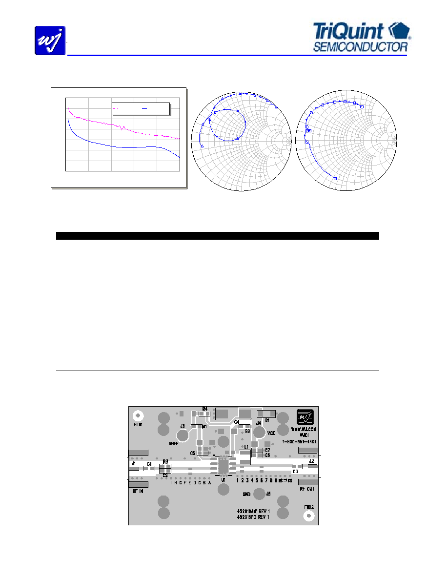
Typical Device Data
S-Parameters (Vcc = +5 V, Icc = 250 mA, T = 25 °C T = 25 °C, calibrated to device leads)
0
0.5
1
1.5
2
2.5
Frequency (GHz)
Gain and Maximum Stable Gain
0
5
10
15
20
25
30
35
Ga
in
(
d
B
)
DB(GMax)
DB(|S[2,1]|)
0
1.
0
1.0
-1.0
1
0.0
10.0
-1
0.
0
5.
0
5.
0
-5
.0
2.
0
2
.
0
-
2
.
0
3.
0
3.
0
-3
.0
4.
0
4.
0
-4
.0
0.
2
0.
2
-0
.2
0.
4
0.4
-
0.
4
0.
6
0
.
6
-
0
.
6
0.
8
0
.
8
-
0
.
8
S11
Swp Max
5.05GHz
Swp Min
0.05GHz
0
1.0
-1.0
10.0
-1
0.
0
5.0
5.
0
-5
.0
2.0
2
.
0
-
2
.
0
3.0
3.
0
-3
.0
4.0
4.
0
-4
.0
0.2
0.
2
-0
.2
0.4
0.
4
-0
.4
0.6
0
.
6
-
0
.
6
0.8
0
.
8
-
0
.
8
S22
Swp Max
5.05GHz
Swp Min
0.05GHz
Notes:
The gain for the unmatched device in 50-ohm system is shown as the trace in black color. For a tuned circuit for a particular frequency,
it is expected that actual gain will be higher, up to the maximum stable gain. The maximum stable gain is shown in the dashed red line.
The return loss plots are shown from 50 – 5050 MHz, with markers placed at 0.5 – 5.05 GHz in 0.5 GHz increments.
S-Parameters (Vcc = +5 V, Icc = 250 mA, T = 25 °C, unmatched 50 ohm system, calibrated to device leads)
Freq (MHz)
S11 (dB)
S11 (ang)
S21 (dB)
S21 (ang)
S12 (dB)
S12 (ang)
S22 (dB)
S22 (ang)
50
-2.11
-172.90
25.10
133.84
-36.03
31.44
-2.06
-105.55
100
-1.59
-178.94
21.15
126.67
-35.22
15.04
-2.73
-138.75
200
-1.51
173.71
17.75
124.19
-34.29
7.30
-2.80
-160.44
400
-1.45
163.84
15.23
111.50
-34.45
-2.16
-2.73
-174.00
600
-1.58
153.68
13.69
98.94
-33.58
-2.99
-1.96
-179.13
800
-1.78
144.31
12.77
84.57
-32.84
-12.80
-1.68
172.00
1000
-1.96
134.21
11.94
69.70
-32.77
-18.76
-1.85
166.98
1200
-2.46
123.44
11.36
55.57
-31.79
-30.73
-2.14
164.05
1400
-3.30
111.21
11.17
40.93
-31.12
-45.14
-2.30
163.07
1600
-4.70
92.57
11.39
22.80
-30.30
-61.92
-2.52
164.84
1800
-8.15
78.58
11.64
1.64
-29.47
-83.99
-2.43
164.25
2000
-19.01
93.29
11.51
-25.24
-29.31
-112.79
-1.84
162.38
2200
-9.59
177.56
10.35
-55.97
-30.51
-150.45
-1.22
155.68
2400
-4.09
159.30
7.87
-83.78
-32.59
177.62
-1.06
147.58
2600
-1.99
141.65
4.95
-105.90
-33.96
137.14
-1.07
139.74
2800
-1.12
127.57
1.97
-122.86
-34.68
109.27
-1.19
132.15
3000
-0.72
116.11
-0.88
-136.93
-35.64
81.83
-1.44
125.05
Device S-parameters are available for download from the website at: http://www.wj.com
Application Circuit PC Board Layout
Circuit Board Material: .014” Getek, 4 - layer, 1 oz copper, Microstrip line details: width = .026”, spacing = .026”
The silk screen markers ‘A’, ‘B’, ‘C’, etc. and ‘1’, ‘2’, ‘3’, etc. are used as placemarkers for the input and output tuning
shunt capacitors – C8 and C9. The markers and vias are spaced in .050” increments.
相關(guān)PDF資料 |
PDF描述 |
|---|---|
| AH115-S8 | 1800 MHz - 2300 MHz RF/MICROWAVE NARROW BAND MEDIUM POWER AMPLIFIER |
| AH115-S8 | 1800 MHz - 2300 MHz RF/MICROWAVE NARROW BAND MEDIUM POWER AMPLIFIER |
| AH115 | 1800 MHz - 2300 MHz RF/MICROWAVE NARROW BAND MEDIUM POWER AMPLIFIER |
| AH115 | 1800 MHz - 2300 MHz RF/MICROWAVE NARROW BAND MEDIUM POWER AMPLIFIER |
| AH116-S8G | 800 MHz - 1000 MHz RF/MICROWAVE WIDE BAND MEDIUM POWER AMPLIFIER |
相關(guān)代理商/技術(shù)參數(shù) |
參數(shù)描述 |
|---|---|
| AH115-S8-G | 制造商:TriQuint Semiconductor 功能描述:RF & MW DRIVER AMPLIFIER 制造商:TriQuint Semiconductor 功能描述:RF Amp Chip Single GP 2.3GHz 8-Pin SOIC |
| AH115-S8PCB1960 | 功能描述:射頻開發(fā)工具 1960MHz Eval Brd 14.4dB Gain RoHS:否 制造商:Taiyo Yuden 產(chǎn)品:Wireless Modules 類型:Wireless Audio 工具用于評(píng)估:WYSAAVDX7 頻率: 工作電源電壓:3.4 V to 5.5 V |
| AH115-S8PCB2140 | 功能描述:射頻開發(fā)工具 2140MHz Eval Brd 14.4dB Gain RoHS:否 制造商:Taiyo Yuden 產(chǎn)品:Wireless Modules 類型:Wireless Audio 工具用于評(píng)估:WYSAAVDX7 頻率: 工作電源電壓:3.4 V to 5.5 V |
| AH115-S8TRG | 制造商:TriQuint Semiconductor 功能描述:RF & MW DRIVER AMPLIFIER |
| AH116 | 制造商:未知廠家 制造商全稱:未知廠家 功能描述:InGaP HBT Amplifiers |
發(fā)布緊急采購(gòu),3分鐘左右您將得到回復(fù)。