- 您現(xiàn)在的位置:買賣IC網(wǎng) > PDF目錄166094 > AH110-89G (TRIQUINT SEMICONDUCTOR INC) 50 MHz - 2000 MHz RF/MICROWAVE WIDE BAND MEDIUM POWER AMPLIFIER PDF資料下載
參數(shù)資料
| 型號: | AH110-89G |
| 廠商: | TRIQUINT SEMICONDUCTOR INC |
| 元件分類: | 放大器 |
| 英文描述: | 50 MHz - 2000 MHz RF/MICROWAVE WIDE BAND MEDIUM POWER AMPLIFIER |
| 封裝: | GREEN, TO-243C, SOT-89, SMT, 3 PIN |
| 文件頁數(shù): | 2/5頁 |
| 文件大小: | 260K |
| 代理商: | AH110-89G |
Specifications and information are subject to change without notice
TriQuint Semiconductor Inc Phone 1-503-615-9000 FAX: 503-615-8900 e-mail: info-sales@tqs.com Web site: www.TriQuint.com
Page 2 of 5 April 2010
AH110
0.2 Watt, High Linearity InGaP HBT Amplifier
Typical Device Data
S-parameters (Vdevice = +5V, Icc = 100 mA, 25 °C, unmatched 50 ohm system)
0
0.5
1
1.5
2
Frequency (GHz)
Gain / Maximum Stable Gain
10
15
20
25
30
G
a
in
(d
B
)
DB(|S[2,1]|)
DB(GMax)
0
1
.
0
1
.
0
-
1
.
0
1
0
.
0
10.
0
-1
0.
0
5
.
0
5.
0
-5
.0
2
.
0
2
.
0
-
2
.
0
3
.
0
3
.
0
-
3
.
0
4
.
0
4.
0
- 4
.0
0
.
2
0.
2
-0
.2
0
.
4
0
.
4
-
0
.
4
0
.
6
0
.
6
-
0
.
6
0
.
8
0
.
8
-
0
.
8
S11
Swp Max
2.01283GHz
Swp Min
0.01483GHz
0
1
.
0
1
.
0
-
1
.
0
1
0
.
0
10.
0
-1
0.
0
5
.
0
5.
0
-5
.0
2
.
0
2
.
0
-
2
.
0
3
.
0
3
.
0
-
3
.
0
4
.
0
4.
0
-4
.0
0
.
2
0.
2
- 0
.2
0
.
4
0
.
4
-
0
.
4
0
.
6
0
.
6
-
0
.
6
0
.
8
0
.
8
-
0
.
8
S22
Swp Max
2.01283GHz
Swp Min
0.01483GHz
Notes:
The gain for the unmatched device in 50 ohm system is shown as the trace in blue color. For a tuned circuit for a particular frequency, it is expected that
actual gain will be higher, up to the maximum stable gain. The maximum stable gain is shown in the dashed red line.
The impedance plots are shown from 50 – 2500 MHz, with markers placed at 0.25 – 2 GHz in 0.25 GHz increments.
S-Parameters (Vdevice = +5 V, Icc = 100 mA, T = 25 °C, unmatched 50 ohm system, calibrated to device leads)
Freq (MHz)
S11 (dB)
S11 (ang)
S21 (dB)
S21 (ang)
S12 (dB)
S12 (ang)
S22 (dB)
S22 (ang)
50
-5.21
-158.20
27.34
141.96
-32.11
16.29
-6.58
-132.30
100
-4.92
-170.08
25.32
144.95
-31.61
9.45
-7.49
-157.02
200
-4.72
-177.73
24.15
138.50
-31.37
6.88
-7.96
-171.72
400
-4.31
173.22
22.43
118.30
-30.63
7.98
-8.46
178.73
600
-4.10
163.26
20.91
100.56
-30.32
5.52
-8.81
174.06
800
-4.19
152.57
19.68
85.04
-29.78
2.65
-9.07
171.40
1000
-4.63
140.41
18.82
69.98
-29.74
-2.18
-9.12
169.67
1200
-5.64
126.43
18.35
54.85
-29.31
-11.26
-8.95
170.98
1400
-7.84
109.08
18.13
38.12
-29.86
-26.72
-8.04
175.14
1600
-13.52
83.27
18.12
17.54
-31.16
-52.52
-6.16
179.09
1800
-19.89
-85.25
17.78
-7.75
-34.99
-105.12
-3.43
176.43
2000
-6.99
-131.98
16.44
-37.07
-34.48
161.53
-1.36
164.56
2200
-2.84
-160.75
14.09
-64.48
-29.33
106.22
-0.69
149.67
2400
-1.18
177.40
10.90
-86.11
-26.64
75.52
-0.93
136.25
2500
-0.78
167.87
9.28
-96.04
-25.96
66.16
-1.28
130.16
Device S-parameters are available for download off of the website at: http://www.wj.com
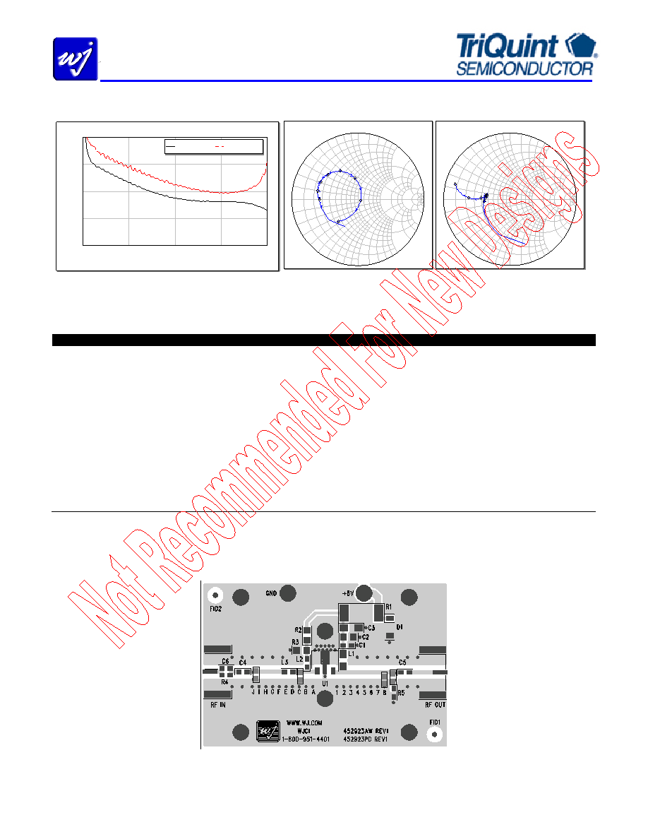
Application Circuit PC Board Layout
Circuit Board Material: .014” Getek, 4-layer, 1 oz copper, Microstrip line details: width = .026”, spacing = .026”
The silk screen markers ‘A’, ‘B’, ‘C’, etc. and ‘1’, ‘2’, ‘3’, etc. are used as placemarkers for the input and output tuning shunt capacitors.
The markers and vias are spaced in .050” increments.
C7/C8 are for 900 MHz matching circuits and C9/C12 are for 1900 MHz matching circuits.
C8
C7
C9
C12
相關PDF資料 |
PDF描述 |
|---|---|
| AH1464 | SNAP ACTING/LIMIT SWITCH, SPDT, MOMENTARY, 2.6mm, THROUGH HOLE-STRAIGHT |
| AH1682 | SNAP ACTING/LIMIT SWITCH, SPDT, MOMENTARY, 2.65mm, PANEL MOUNT |
| AH1482 | SNAP ACTING/LIMIT SWITCH, SPDT, MOMENTARY, 2.65mm, THROUGH HOLE-STRAIGHT |
| AH152-82 | VHF-KA BAND, 0.62 pF, 30 V, GALLIUM ARSENIDE, ABRUPT VARIABLE CAPACITANCE DIODE |
| AH160-84 | VHF-KA BAND, 0.62 pF, 45 V, GALLIUM ARSENIDE, ABRUPT VARIABLE CAPACITANCE DIODE |
相關代理商/技術參數(shù) |
參數(shù)描述 |
|---|---|
| AH110-89PCB1900 | 功能描述:射頻開發(fā)工具 1900MHz Eval Brd 17.5dB Gain RoHS:否 制造商:Taiyo Yuden 產(chǎn)品:Wireless Modules 類型:Wireless Audio 工具用于評估:WYSAAVDX7 頻率: 工作電源電壓:3.4 V to 5.5 V |
| AH110-89PCB900 | 功能描述:射頻開發(fā)工具 900MHz Eval Brd 20.5dB Gain RoHS:否 制造商:Taiyo Yuden 產(chǎn)品:Wireless Modules 類型:Wireless Audio 工具用于評估:WYSAAVDX7 頻率: 工作電源電壓:3.4 V to 5.5 V |
| AH110-RFID | 制造商:WJCI 制造商全稱:WJCI 功能描述:0.2 Watt, High Linearity InGaP HBT Amplifier |
| AH11-1 | 制造商:未知廠家 制造商全稱:未知廠家 功能描述:Analog IC |
| AH11109 | 制造商:Panasonic Electric Works 功能描述: |
發(fā)布緊急采購,3分鐘左右您將得到回復。