- 您現(xiàn)在的位置:買賣IC網(wǎng) > PDF目錄4539 > AGL030V5-VQG100I (Microsemi SoC)IC FPGA 1KB FLASH 30K 100-VQFP PDF資料下載
參數(shù)資料
| 型號(hào): | AGL030V5-VQG100I |
| 廠商: | Microsemi SoC |
| 文件頁(yè)數(shù): | 35/250頁(yè) |
| 文件大小: | 0K |
| 描述: | IC FPGA 1KB FLASH 30K 100-VQFP |
| 標(biāo)準(zhǔn)包裝: | 90 |
| 系列: | IGLOO |
| 邏輯元件/單元數(shù): | 768 |
| 輸入/輸出數(shù): | 77 |
| 門數(shù): | 30000 |
| 電源電壓: | 1.425 V ~ 1.575 V |
| 安裝類型: | 表面貼裝 |
| 工作溫度: | -40°C ~ 85°C |
| 封裝/外殼: | 100-TQFP |
| 供應(yīng)商設(shè)備封裝: | 100-VQFP(14x14) |
第1頁(yè)第2頁(yè)第3頁(yè)第4頁(yè)第5頁(yè)第6頁(yè)第7頁(yè)第8頁(yè)第9頁(yè)第10頁(yè)第11頁(yè)第12頁(yè)第13頁(yè)第14頁(yè)第15頁(yè)第16頁(yè)第17頁(yè)第18頁(yè)第19頁(yè)第20頁(yè)第21頁(yè)第22頁(yè)第23頁(yè)第24頁(yè)第25頁(yè)第26頁(yè)第27頁(yè)第28頁(yè)第29頁(yè)第30頁(yè)第31頁(yè)第32頁(yè)第33頁(yè)第34頁(yè)當(dāng)前第35頁(yè)第36頁(yè)第37頁(yè)第38頁(yè)第39頁(yè)第40頁(yè)第41頁(yè)第42頁(yè)第43頁(yè)第44頁(yè)第45頁(yè)第46頁(yè)第47頁(yè)第48頁(yè)第49頁(yè)第50頁(yè)第51頁(yè)第52頁(yè)第53頁(yè)第54頁(yè)第55頁(yè)第56頁(yè)第57頁(yè)第58頁(yè)第59頁(yè)第60頁(yè)第61頁(yè)第62頁(yè)第63頁(yè)第64頁(yè)第65頁(yè)第66頁(yè)第67頁(yè)第68頁(yè)第69頁(yè)第70頁(yè)第71頁(yè)第72頁(yè)第73頁(yè)第74頁(yè)第75頁(yè)第76頁(yè)第77頁(yè)第78頁(yè)第79頁(yè)第80頁(yè)第81頁(yè)第82頁(yè)第83頁(yè)第84頁(yè)第85頁(yè)第86頁(yè)第87頁(yè)第88頁(yè)第89頁(yè)第90頁(yè)第91頁(yè)第92頁(yè)第93頁(yè)第94頁(yè)第95頁(yè)第96頁(yè)第97頁(yè)第98頁(yè)第99頁(yè)第100頁(yè)第101頁(yè)第102頁(yè)第103頁(yè)第104頁(yè)第105頁(yè)第106頁(yè)第107頁(yè)第108頁(yè)第109頁(yè)第110頁(yè)第111頁(yè)第112頁(yè)第113頁(yè)第114頁(yè)第115頁(yè)第116頁(yè)第117頁(yè)第118頁(yè)第119頁(yè)第120頁(yè)第121頁(yè)第122頁(yè)第123頁(yè)第124頁(yè)第125頁(yè)第126頁(yè)第127頁(yè)第128頁(yè)第129頁(yè)第130頁(yè)第131頁(yè)第132頁(yè)第133頁(yè)第134頁(yè)第135頁(yè)第136頁(yè)第137頁(yè)第138頁(yè)第139頁(yè)第140頁(yè)第141頁(yè)第142頁(yè)第143頁(yè)第144頁(yè)第145頁(yè)第146頁(yè)第147頁(yè)第148頁(yè)第149頁(yè)第150頁(yè)第151頁(yè)第152頁(yè)第153頁(yè)第154頁(yè)第155頁(yè)第156頁(yè)第157頁(yè)第158頁(yè)第159頁(yè)第160頁(yè)第161頁(yè)第162頁(yè)第163頁(yè)第164頁(yè)第165頁(yè)第166頁(yè)第167頁(yè)第168頁(yè)第169頁(yè)第170頁(yè)第171頁(yè)第172頁(yè)第173頁(yè)第174頁(yè)第175頁(yè)第176頁(yè)第177頁(yè)第178頁(yè)第179頁(yè)第180頁(yè)第181頁(yè)第182頁(yè)第183頁(yè)第184頁(yè)第185頁(yè)第186頁(yè)第187頁(yè)第188頁(yè)第189頁(yè)第190頁(yè)第191頁(yè)第192頁(yè)第193頁(yè)第194頁(yè)第195頁(yè)第196頁(yè)第197頁(yè)第198頁(yè)第199頁(yè)第200頁(yè)第201頁(yè)第202頁(yè)第203頁(yè)第204頁(yè)第205頁(yè)第206頁(yè)第207頁(yè)第208頁(yè)第209頁(yè)第210頁(yè)第211頁(yè)第212頁(yè)第213頁(yè)第214頁(yè)第215頁(yè)第216頁(yè)第217頁(yè)第218頁(yè)第219頁(yè)第220頁(yè)第221頁(yè)第222頁(yè)第223頁(yè)第224頁(yè)第225頁(yè)第226頁(yè)第227頁(yè)第228頁(yè)第229頁(yè)第230頁(yè)第231頁(yè)第232頁(yè)第233頁(yè)第234頁(yè)第235頁(yè)第236頁(yè)第237頁(yè)第238頁(yè)第239頁(yè)第240頁(yè)第241頁(yè)第242頁(yè)第243頁(yè)第244頁(yè)第245頁(yè)第246頁(yè)第247頁(yè)第248頁(yè)第249頁(yè)第250頁(yè)
IGLOO Low Power Flash FPGAs
Revision 23
1-7
The inputs of the six CCC blocks are accessible from the FPGA core or from one of several inputs
located near the CCC that have dedicated connections to the CCC block.
The CCC block has these key features:
Wide input frequency range (fIN_CCC) = 1.5 MHz up to 250 MHz
Output frequency range (fOUT_CCC) = 0.75 MHz up to 250 MHz
2 programmable delay types for clock skew minimization
Clock frequency synthesis (for PLL only)
Additional CCC specifications:
Internal phase shift = 0°, 90°, 180°, and 270°. Output phase shift depends on the output divider
configuration (for PLL only).
Output duty cycle = 50% ± 1.5% or better (for PLL only)
Low output jitter: worst case < 2.5% × clock period peak-to-peak period jitter when single global
network used (for PLL only)
Maximum acquisition time is 300 s (for PLL only)
Exceptional tolerance to input period jitter—allowable input jitter is up to 1.5 ns (for PLL only)
Four precise phases; maximum misalignment between adjacent phases of 40 ps × 250 MHz /
fOUT_CCC (for PLL only)
Global Clocking
IGLOO devices have extensive support for multiple clocking domains. In addition to the CCC and PLL
support described above, there is a comprehensive global clock distribution network.
Each VersaTile input and output port has access to nine VersaNets: six chip (main) and three quadrant
global networks. The VersaNets can be driven by the CCC or directly accessed from the core via
multiplexers (MUXes). The VersaNets can be used to distribute low-skew clock signals or for rapid
distribution of high-fanout nets.
I/Os with Advanced I/O Standards
The IGLOO family of FPGAs features a flexible I/O structure, supporting a range of voltages (1.2 V, 1.5 V,
1.8 V, 2.5 V, 3.0 V wide range, and 3.3 V). IGLOO FPGAs support many different I/O standards—single-
ended and differential.
The I/Os are organized into banks, with two or four banks per device. The configuration of these banks
determines the I/O standards supported (Table 1-1).
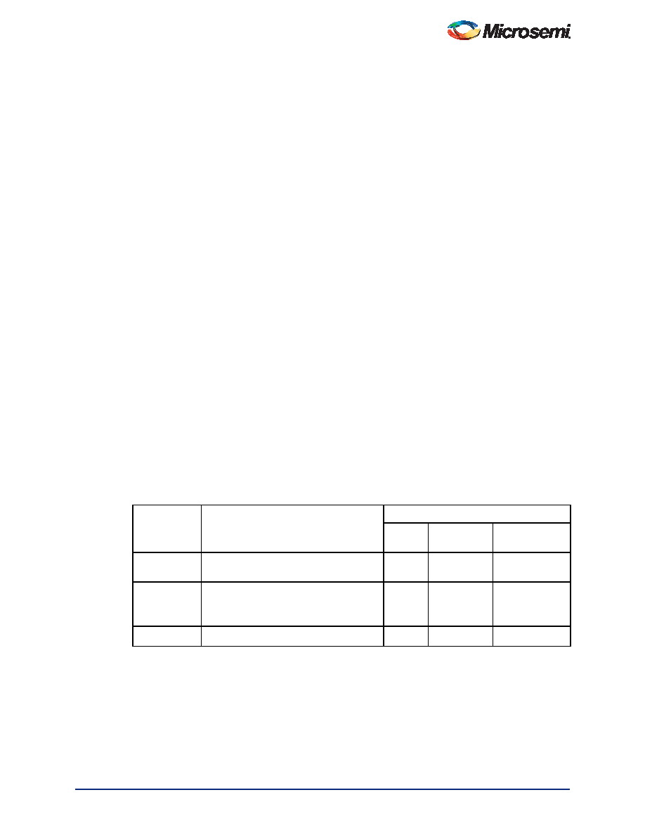
Table 1-1 I/O Standards Supported
I/O Bank Type
Device and Bank Location
I/O Standards Supported
LVTTL/
LVCMOS
PCI/PCI-X
LVPECL, LVDS,
B-LVDS, M-LVDS
Advanced
East and west banks of AGL250 and larger
devices
Standard Plus North and south banks of AGL250 and
larger devices
All banks of AGL060 and AGL125K
Not supported
Standard
All banks of AGL015 and AGL030
Not supported
相關(guān)PDF資料 |
PDF描述 |
|---|---|
| AGLN030V2-ZVQG100 | IC FPGA NANO 1KB 30K 100VQFP |
| A3P030-VQG100I | IC FPGA 1KB FLASH 30K 100-VQFP |
| AGLN030V5-ZVQ100I | IC FPGA NANO 1KB 30K 100VQFP |
| ABM44DRTH | CONN EDGECARD 88POS DIP .156 SLD |
| ASM24DRMD | CONN EDGECARD 48POS .156 WW |
相關(guān)代理商/技術(shù)參數(shù) |
參數(shù)描述 |
|---|---|
| AGL030V5-VQG144 | 制造商:ACTEL 制造商全稱:Actel Corporation 功能描述:IGLOO Low-Power Flash FPGAs with Flash Freeze Technology |
| AGL030V5-VQG144ES | 制造商:ACTEL 制造商全稱:Actel Corporation 功能描述:IGLOO Low-Power Flash FPGAs with Flash Freeze Technology |
| AGL030V5-VQG144I | 制造商:ACTEL 制造商全稱:Actel Corporation 功能描述:IGLOO Low-Power Flash FPGAs with Flash Freeze Technology |
| AGL030V5-VQG144PP | 制造商:ACTEL 制造商全稱:Actel Corporation 功能描述:IGLOO Low-Power Flash FPGAs with Flash Freeze Technology |
| AGL032-100-300 | 制造商:ROEBUCK 功能描述:JSP GOGGLE FLIP UP WELDERS GRN |
發(fā)布緊急采購(gòu),3分鐘左右您將得到回復(fù)。