- 您現在的位置:買賣IC網 > PDF目錄374047 > ADV7302AKST (ANALOG DEVICES INC) Sand Paper; Abrasive Grade:A VFN; Color:Maroon; Pack Quantity:6; Roll Length:30ft; Width:2" PDF資料下載
參數資料
| 型號: | ADV7302AKST |
| 廠商: | ANALOG DEVICES INC |
| 元件分類: | 顏色信號轉換 |
| 英文描述: | Sand Paper; Abrasive Grade:A VFN; Color:Maroon; Pack Quantity:6; Roll Length:30ft; Width:2" |
| 中文描述: | COLOR SIGNAL ENCODER, PQFP64 |
| 封裝: | PLASTIC, MS-026BCD, LQFP-64 |
| 文件頁數: | 12/68頁 |
| 文件大小: | 1177K |
| 代理商: | ADV7302AKST |
第1頁第2頁第3頁第4頁第5頁第6頁第7頁第8頁第9頁第10頁第11頁當前第12頁第13頁第14頁第15頁第16頁第17頁第18頁第19頁第20頁第21頁第22頁第23頁第24頁第25頁第26頁第27頁第28頁第29頁第30頁第31頁第32頁第33頁第34頁第35頁第36頁第37頁第38頁第39頁第40頁第41頁第42頁第43頁第44頁第45頁第46頁第47頁第48頁第49頁第50頁第51頁第52頁第53頁第54頁第55頁第56頁第57頁第58頁第59頁第60頁第61頁第62頁第63頁第64頁第65頁第66頁第67頁第68頁
REV. A
–12–
ADV7302A/ADV7303A
CAUTION
ESD (electrostatic discharge) sensitive device. Electrostatic charges as high as 4000 V readily
accumulate on the human body and test equipment and can discharge without detection. Although the
ADV7302A/ADV7303A features proprietary ESD protection circuitry, permanent damage may occur
on devices subjected to high energy electrostatic discharges. Therefore, proper ESD precautions are
recommended to avoid performance degradation or loss of functionality.
ABSOLUTE MAXIMUM RATINGS
*
V
AA
to AGND . . . . . . . . . . . . . . . . . . . . . . . . +3.0 V to –0.3 V
V
DD
to GND . . . . . . . . . . . . . . . . . . . . . . . . . +3.0 V to –0.3 V
V
DD_IO
to IO_GND . . . . . . . . . . . . . –0.3 V to V
DD_IO
+ 0.3 V
Ambient Operating Temperature (T
A
) . . . . . . . 0
°
C to +70
°
C
Storage Temperature (T
S
) . . . . . . . . . . . . . . –65
°
C to +150
°
C
Infrared Reflow Soldering (20 sec) . . . . . . . . . . . . . . . . 260
°
C
*
Stresses above those listed under Absolute Maximum Ratings may cause perma-
nent damage to the device. This is a stress rating only; functional operation of the
device at these or any other conditions above those listed in the operational
sections of this specification is not implied. Exposure to absolute maximum rating
conditions for extended periods may affect device reliability.
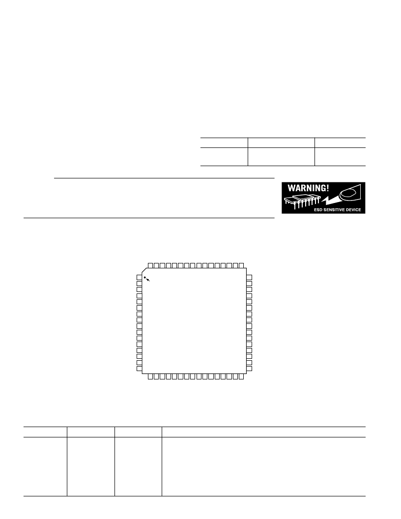
PIN CONFIGURATION
1
2
3
4
5
6
7
8
9
10
11
12
13
14
15
16
PIN 1
TOP VIEW
(Not to Scale)
V
DD_IO
GND_IO
GND_IO
48
47
46
45
44
43
42
41
40
39
38
37
36
35
34
33
49
50
51
52
53
54
55
56
57
58
59
60
61
62
63
64
32
C
31
R
30
C
29
C
28
C
27
C
26
C
25
P
24
P
23
P
22
S
21
S
20
A
19
I
2
C
18
C
17
C
Y0
Y1
Y2
Y3
Y4
Y5
V
DD
DGND
Y6
Y7
GND_IO
GND_IO
C0
S_BLANK
R
SET1
V
REF
COMP1
DAC A
DAC B
DAC C
V
AA
AGND
DAC D
DAC E
DAC F
COMP2
R
SET2
EXT_LF
RESET
G
C
S
S
S
S
S
D
V
D
S
S
S
G
G
S
S
ADV7302A/ADV7303A
The ADV7302A/ADV7303A is a lead-free environmentally
friendly product. It is manufactured using the most up-to-date
materials and processes. The coating on the leads of each device
is 100% pure tin electroplate. The device is suitable for lead-free
applications and is able to withstand surface-mount soldering at
up to 255
°
C (
±
5
°
C). In addition, it is backward compatible with
conventional tin-lead soldering processes. This means that the
electroplated tin coating can be soldered with tin-lead solder
pastes at conventional reflow temperatures of 220
°
C to 235
°
C.
PIN FUNCTION DESCRIPTIONS
Pin No.
Mnemonic
Input/Output
Function
1
4–9, 12, 13
V
DD_IO
Y0–Y7
P
I
Power Supply for Digital Inputs and Outputs
8-Bit Progressive Scan/HDTV Input Port for Y Data. The LSBs are set up on
Pins Y0 and Y1. In default mode, the input on this port is output on DAC D.
8-Bit Progressive Scan/HDTV Input Port for CrCb Color Data in 4:2:2 Input
Mode. In 4:4:4 Input Mode, this input port is used for the Cb (Blue/U) data.
The LSBs are set up on Pins C0 and C1. In default mode, the input on this
port is output on DAC E.
16–18, 26–30
C0–C7
I
ORDERING GUIDE
Model
Package Description
Package Option
ADV7302AKST
ADV7303AKST
Plastic Quad Flatpack
Plastic Quad Flatpack
ST-64B
ST-64B
THERMAL CHARACTERISTICS
θ
JC
= 11
°
C/W
θ
JA
= 47
°
C/W
相關PDF資料 |
PDF描述 |
|---|---|
| ADV7303A | Sand Paper; Abrasive Grade:A VFN; Color:Maroon; Pack Quantity:4; Roll Length:30ft; Width:3" |
| ADV7303AKST | Sand Paper; Abrasive Grade:T; Color:White; Pack Quantity:3; Roll Length:30ft; Width:4" |
| ADV7310 | Multiformat 216 MHz Video Encoder with Six NSV 12-Bit DACs |
| ADV7310KST | Multiformat 216 MHz Video Encoder with Six NSV 12-Bit DACs |
| ADV7311 | Multiformat 216 MHz Video Encoder with Six NSV 12-Bit DACs |
相關代理商/技術參數 |
參數描述 |
|---|---|
| ADV7303A | 制造商:AD 制造商全稱:Analog Devices 功能描述:Multiformat SD, Progressive Scan/HDTV Video Encoder with Six 11-Bit DACs |
| ADV7303AKST | 制造商:Rochester Electronics LLC 功能描述:150MHZ HD 108MHZ PROG SCAN 11BIT ENC I.C - Bulk 制造商:Analog Devices 功能描述: |
| ADV73045701 | 制造商:LG Corporation 功能描述:Frame Assembly |
| ADV73045702 | 制造商:LG Corporation 功能描述:Frame Assembly |
| ADV73045703 | 制造商:LG Corporation 功能描述:Frame Assembly |
發(fā)布緊急采購,3分鐘左右您將得到回復。