- 您現(xiàn)在的位置:買賣IC網(wǎng) > PDF目錄374046 > ADV7171SU (ANALOG DEVICES INC) Digital PAL/NTSC Video Encoder with 10-Bit SSAF⑩ and Advanced Power Management PDF資料下載
參數(shù)資料
| 型號: | ADV7171SU |
| 廠商: | ANALOG DEVICES INC |
| 元件分類: | 顏色信號轉(zhuǎn)換 |
| 英文描述: | Digital PAL/NTSC Video Encoder with 10-Bit SSAF⑩ and Advanced Power Management |
| 中文描述: | COLOR SIGNAL ENCODER, PQFP44 |
| 封裝: | PLASTIC, TQFP-44 |
| 文件頁數(shù): | 26/55頁 |
| 文件大小: | 754K |
| 代理商: | ADV7171SU |
第1頁第2頁第3頁第4頁第5頁第6頁第7頁第8頁第9頁第10頁第11頁第12頁第13頁第14頁第15頁第16頁第17頁第18頁第19頁第20頁第21頁第22頁第23頁第24頁第25頁當(dāng)前第26頁第27頁第28頁第29頁第30頁第31頁第32頁第33頁第34頁第35頁第36頁第37頁第38頁第39頁第40頁第41頁第42頁第43頁第44頁第45頁第46頁第47頁第48頁第49頁第50頁第51頁第52頁第53頁第54頁第55頁
ADV7170/ADV7171
–26–
REV. 0
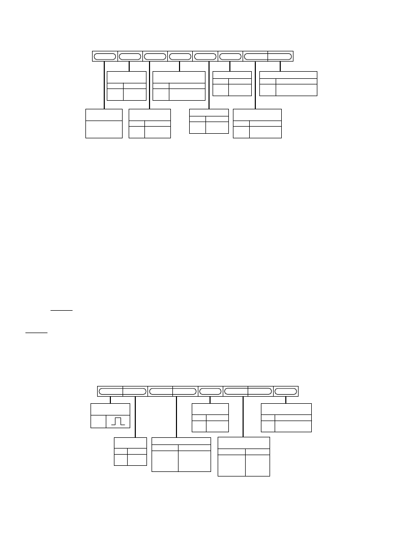
MODE REGISTER 4 MR4 (MR47–MR40)
(Address (SR4–SR0) = 04H)
Mode Register 4 is a 8-bit-wide register.
Figure 42 shows the various operations under the control of
Mode Register 4.
MR4 BIT DESCRIPTION
Output Select (MR40)
This bit specifies if the part is in composite video or RGB/YUV
mode. Note that in RGB/YUV mode the composite signal is
still available.
RGB/YUV Control (MR41)
This bit enables the output from the RGB DACs to be set to
YUV output video standard.
RGB Sync (MR42)
This bit is used to set up the RGB outputs with the sync infor-
mation encoded on all RGB outputs.
VSYNC
_3H Control (MR43)
When this bit is enabled (“1”) in slave mode, it is possible to
drive the
VSYNC
active low input for 2.5 lines in PAL mode
and 3 lines in NTSC mode. When this bit is enabled in mas-
ter mode, the ADV7170/ADV7171 outputs an active low
VSYNC
signal for 3 lines in NTSC mode and 2.5 lines in PAL
mode.
MR41
MR40
MR47
MR42
MR44
MR43
MR45
MR46
OUTPUT SELECT
MR40
0
YC OUTPUT
RGB/YUV OUTPUT
RGB SYNC
MR42
0
1
DISABLE
ENABLE
PEDESTAL
CONTROL
0
1
PEDESTAL OFF
PEDESTAL ON
MR44
SLEEP MODE
CONTROL
MR46
0
1
DISABLE
ENABLE
ACTIVE VIDEO
FILTER CONTROL
MR45
0
1
ENABLE
DISABLE
MR47
(0)
ZERO SHOULD
BE WRITTEN TO
THIS BIT
VSYNC
_3H
MR43
0
1
DISABLE
ENABLE
RGB/YUV
CONTROL
0
1
RGB OUTPUT
YUV OUTPUT
MR41
Figure 42. Mode Register 4
Pedestal Control (MR44)
This bit specifies whether a pedestal is to be generated on
the NTSC composite video signal. This bit is invalid if the
ADV7170/ADV7171 is configured in PAL mode.
Active Video Filter Switching (MR45)
This bit controls the filter mode applied outside the active video
portion of the line. This filter ensures that the Sync rise and fall
times are always on spec regardless of which Luma filter is se-
lected. A Logic “1” enables this mode.
Sleep Mode Control (MR46)
When this bit is set (“1”) Sleep Mode is enabled. With this
mode enabled, the ADV7170/ADV7171 power consumption is
reduced to typically 200 nA. The I
2
C registers can be written to
and read from when the ADV7170/ADV7171 is in Sleep
Mode. If MR46 is set to a (“0”) when the device is in Sleep
Mode, the ADV7170/ADV7171 will come out of Sleep Mode
and resume normal operation. Also, if the
RESET
signal is
applied during Sleep Mode the ADV7170/ADV7171 will come
out of Sleep Mode and resume normal operation.
Reserved (MR47)
A Logical 0 should be written to this bit.
TIMING REGISTER 0 (TR07–TR00)
(Address [SR4–SR0] = 07H)
Figure 43 shows the various operations under the control of
Timing Register 0. This register can be read from as well as
written to.
TR01
TR00
TR07
TR02
TR03
TR05
TR06
TR04
TIMING
REGISTER RESET
TR07
BLACK INPUT
CONTROL
TR03
0
1
ENABLE
DISABLE
PIXEL PORT
CONTROL
TR06
0
1
8 BIT
16 BIT
MASTER/SLAVE
CONTROL
TR00
0
1
SLAVE TIMING
MASTER TIMING
LUMA DELAY
0
0
1
1
0
1
0
1
0ns DELAY
74ns DELAY
148ns DELAY
222ns DELAY
TR05 TR04
TIMING MODE
SELECTION
TR02 TR01
0
0
1
1
0
1
0
1
MODE 0
MODE 1
MODE 2
MODE 3
Figure 43. Timing Register 0
相關(guān)PDF資料 |
PDF描述 |
|---|---|
| ADV7171* | Digital PAL/NTSC Video Encoder with 10-Bit SSAF and Advanced Power Management |
| ADV7171 | Digital PAL/NTSC Video Encoder(數(shù)字PAL/NTSC視頻編碼器) |
| ADV7173KST | Digital PAL/NTSC Video Encoder with Six DACs 10 Bits, Color Control and Enhanced Power Management |
| ADV7172KST | Digital PAL/NTSC Video Encoder with Six DACs 10 Bits, Color Control and Enhanced Power Management |
| ADV7172 | Digital PAL/NTSC Video Encoder with Six DACs 10 Bits, Color Control and Enhanced Power Management |
相關(guān)代理商/技術(shù)參數(shù) |
參數(shù)描述 |
|---|---|
| ADV7171WBSZ-REEL | 制造商:AD 制造商全稱:Analog Devices 功能描述:Digital PAL/NTSC Video Encoder |
| ADV7172 | 制造商:AD 制造商全稱:Analog Devices 功能描述:Digital PAL/NTSC Video Encoder with Six DACs 10 Bits, Color Control and Enhanced Power Management |
| ADV7172KST | 制造商:AD 制造商全稱:Analog Devices 功能描述:Digital PAL/NTSC Video Encoder with Six DACs 10 Bits, Color Control and Enhanced Power Management |
| ADV7172KST-REEL | 制造商:Analog Devices 功能描述: |
| ADV7172KSTZ | 制造商:Analog Devices 功能描述: |
發(fā)布緊急采購,3分鐘左右您將得到回復(fù)。