- 您現(xiàn)在的位置:買賣IC網(wǎng) > PDF目錄374039 > ADUC844BCP32-5 (ANALOG DEVICES INC) MicroConverter, Dual 16-Bit/24-Bit ADCs with Embedded 62kB FLASH MCU PDF資料下載
參數(shù)資料
| 型號(hào): | ADUC844BCP32-5 |
| 廠商: | ANALOG DEVICES INC |
| 元件分類: | 微控制器/微處理器 |
| 英文描述: | MicroConverter, Dual 16-Bit/24-Bit ADCs with Embedded 62kB FLASH MCU |
| 中文描述: | 8-BIT, FLASH, 12.58 MHz, MICROCONTROLLER, QCC56 |
| 封裝: | 8 X 8 MM, MO-220-VLLD-2, LFCSP-56 |
| 文件頁(yè)數(shù): | 14/20頁(yè) |
| 文件大小: | 674K |
| 代理商: | ADUC844BCP32-5 |
第1頁(yè)第2頁(yè)第3頁(yè)第4頁(yè)第5頁(yè)第6頁(yè)第7頁(yè)第8頁(yè)第9頁(yè)第10頁(yè)第11頁(yè)第12頁(yè)第13頁(yè)當(dāng)前第14頁(yè)第15頁(yè)第16頁(yè)第17頁(yè)第18頁(yè)第19頁(yè)第20頁(yè)
ADuC844
The 11-bit stack pointer is visable in the SP and SPH SFRs. The SP
SFR is located at 81h as with a standard 8052. The SPH SFR is
located at B7h. The 3 LSBs of this SFR contain the 3 extra bits
necessary to extend the 8-bit stack pointer into an 11-bit stack
pointer.
-14-
REV. PrB
PRELIMINARY TECHNICAL DATA
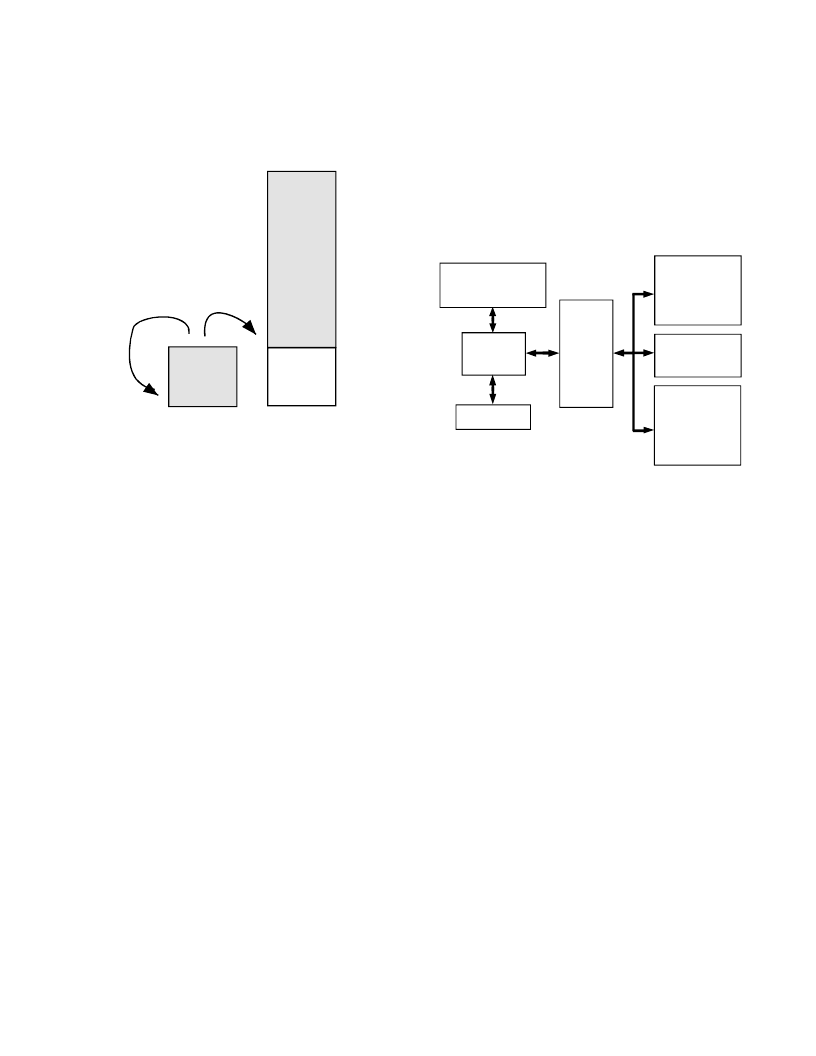
UPPER 1792
BYTES OF
ON-CHIP XRAM
(DATA +STACK
FOR EXSP=1,
DATA ONLY
FOR EXSP=0)
256 BYTES OF
ON-CHIP DATA
RAM
(DATA + STACK)
LOWER 256
BYTES OF
ON-CHIP XRAM
(DATA ONLY)
00H
FFH
100H
00H
07FFH
CFG845.7 = 0
CFG845.7 = 1
Figure 4. Extended Stack Pointer Operation
External Data Memory (External XRAM)
Just like a standard 8051 compatible core the ADuC844 can access
external data memory using a MOVX instruction. The MOVX
instruction automatically outputs the various control strobes required
to access the data memory.
The ADuC844 however, can access up to 16MBytes of extrenal data
memory. This is an enhancement of the 64kBytes external data
memory space available on a standard 8051 compatible core.
The external data memory is discussed in more detail in the
ADuC844 Hardware Design Considerations section.
SPECIAL FUNCTION REGISTERS (SFRs)
The SFR space is mapped into the upper 128 bytes of internal data
memory space and accessed by direct addressing only. It provides an
interface between the CPU and all on chip peripherals. A block
diagram showing the programming model of the ADuC844 via the
SFR area is shown in Figure 5.
All registers except the Program Counter (PC) and the four general-
purpose register banks, reside in the SFR area. The SFR registers
include control, configuration, and data registers that provide an
interface between the CPU and all on-chip peripherals.
128-BYTE
SPECIAL
FUNCTION
REGISTER
AREA
62 KBYTE ELECTRICALLY
REPROGRAMMABLE
NONVOLATILE FLASH/EE
PROGRAM MEMORY
8051-
COMPATIBLE
CORE
OTHER ON-CHIP
PERIPHERALS
TEMP SENSOR
CURRENT SOURCES
12-BIT DAC
SERIAL I/O
WDT, PSM
TIC, PLL
DUAL
SIGMA-DELTA
ADCs
4 KBYTE
ELECTRICALLY
REPROGRAMMABLE
NONVOLATILE
FLASH/EE DATA
MEMORY
256 BYTES RAM
2K XRAM
Figure 5. Programming Model
Accumulator SFR (ACC)
ACC is the Accumulator register and is used for math operations
including addition, subtraction, integer multiplication and division,
and Boolean bit manipulations. The mnemonics for accumulator-
specific instructions refer to the Accumulator as A.
B SFR (B)
The B register is used with the ACC for multiplication and division
operations. For other instructions it can be treated as a general-
purpose scratchpad register.
Data Pointer (DPTR)
The Data Pointer is made up of three 8-bit registers, named DPP
(page byte), DPH (high byte) and DPL (low byte). These are used to
provide memory addresses for internal and external code access and
external data access. It may be manipulated as a 16-bit register
(DPTR = DPH, DPL), although INC DPTR instructions will
automatically carry over to DPP, or as three independent 8-bit
registers (DPP, DPH, DPL).
The ADuC844 supports dual data pointers. Refer to the Dual Data
Pointer section later in this datasheet.
Stack Pointer (SP and SPH)
The SP SFR is the stack pointer and is used to hold an internal RAM
address that is called the ‘top of the stack.’ The SP register is
incremented before data is stored during PUSH and CALL
executions. While the Stack may reside anywhere in on-chip RAM,
the SP register is initialized to 07H after a reset. This causes the stack
to begin at location 08H.
As mentioned earlier the ADuC844 offers an extended 11-bit stack
pointer. The 3 extra bits to make up the 11-bit stack pointer are the 3
LSBs of the SPH byte located at B7h. To enable the SPH SFR the
相關(guān)PDF資料 |
PDF描述 |
|---|---|
| ADUC844 | MicroConverter, Dual 16-Bit/24-Bit ADCs with Embedded 62kB FLASH MCU |
| ADUC844BCP62-3 | MicroConverter, Dual 16-Bit/24-Bit ADCs with Embedded 62kB FLASH MCU |
| ADUC844BCP62-5 | MicroConverter, Dual 16-Bit/24-Bit ADCs with Embedded 62kB FLASH MCU |
| ADUC844BCP32-3 | MicroConverter, Dual 16-Bit/24-Bit ADCs with Embedded 62kB FLASH MCU |
| ADUC844BCP8-3 | MicroConverter, Dual 16-Bit/24-Bit ADCs with Embedded 62kB FLASH MCU |
相關(guān)代理商/技術(shù)參數(shù) |
參數(shù)描述 |
|---|---|
| ADUC844BCP62-3 | 制造商:AD 制造商全稱:Analog Devices 功能描述:MicroConverter, Dual 16-Bit/24-Bit ADCs with Embedded 62kB FLASH MCU |
| ADUC844BCP62-5 | 制造商:AD 制造商全稱:Analog Devices 功能描述:MicroConverter, Dual 16-Bit/24-Bit ADCs with Embedded 62kB FLASH MCU |
| ADUC844BCP8-3 | 制造商:AD 制造商全稱:Analog Devices 功能描述:MicroConverter, Dual 16-Bit/24-Bit ADCs with Embedded 62kB FLASH MCU |
| ADUC844BCP8-5 | 制造商:Analog Devices 功能描述:MICROCONVERTER, SINGLE CYCLE FLASH MCU 24BIT +16BIT SIGMA DE - Trays |
| ADUC844BS62-3 | 制造商:AD 制造商全稱:Analog Devices 功能描述:MicroConverter, Dual 16-Bit/24-Bit ADCs with Embedded 62kB FLASH MCU |
發(fā)布緊急采購(gòu),3分鐘左右您將得到回復(fù)。