- 您現(xiàn)在的位置:買賣IC網(wǎng) > PDF目錄223311 > ADS7808U (TEXAS INSTRUMENTS INC) 1-CH 12-BIT SUCCESSIVE APPROXIMATION ADC, SERIAL ACCESS, PDSO20 PDF資料下載
參數(shù)資料
| 型號: | ADS7808U |
| 廠商: | TEXAS INSTRUMENTS INC |
| 元件分類: | ADC |
| 英文描述: | 1-CH 12-BIT SUCCESSIVE APPROXIMATION ADC, SERIAL ACCESS, PDSO20 |
| 封裝: | 0.300 INCH, GREEN, PLASTIC, SOIC-20 |
| 文件頁數(shù): | 12/17頁 |
| 文件大小: | 468K |
| 代理商: | ADS7808U |
ADS7808
4
SBAS018A
www.ti.com
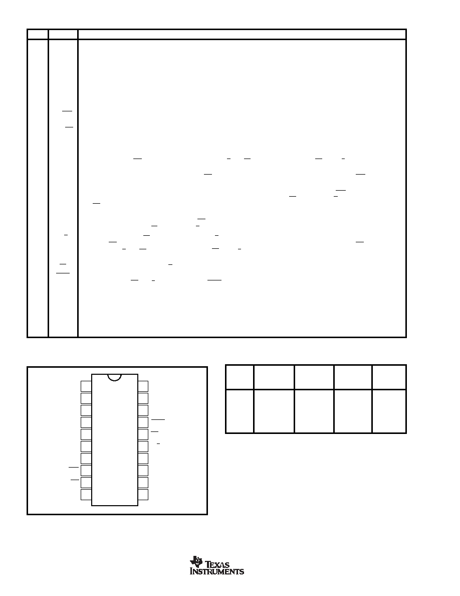
PIN #
NAME
DESCRIPTION
PIN ASSIGNMENTS
PIN CONFIGURATION
V
DIG
V
ANA
PWRD
BUSY
CS
R/C
TAG
DATA
DATACLK
SYNC
R1
IN
AGND1
R2
IN
R3
IN
CAP
REF
AGND2
SB/BTC
EXT/INT
DGND
1
2
3
4
5
6
7
8
9
10
20
19
18
17
16
15
14
13
12
11
ADS7808
ANALOG
CONNECT R1IN
CONNECT R2IN
INPUT
VIA 200
VIA 100
CONNECT R3IN
RANGE
TO
IMPEDANCE
±10V
VIN
AGND
CAP
22.9k
±5V
AGND
VIN
CAP
13.3k
±3.33
VIN
CAP
10.7k
0V to 10V
AGND
VIN
AGND
13.3k
0V to 5V
AGND
VIN
10.0k
0V to 4V
VIN
AGND
VIN
10.7k
TABLE I. Input Range Connections. See Figure 4 for
complete information.
1R1IN
Analog Input. See Table I and Figure 4 for input range connections.
2
AGND1
Analog Ground. Used internally as ground reference point. Minimal current flow.
3R2IN
Analog Input. See Table I and Figure 4 for input range connections.
4R3IN
Analog Input. See Table I and Figure 4 for input range connections.
5
CAP
Reference Buffer Capacitor. 2.2
F Tantalum to ground.
6
REF
Reference Input/Output. Outputs internal 2.5V reference. Can also be driven by external system reference. In both cases,
bypass to ground with a 2.2
F Tantalum capacitor.
7
AGND2
Analog Ground.
8
SB/BTC
Select Straight Binary or Binary Two’s Complement data output format. If HIGH, data will be output in a Straight Binary format. If
LOW, data will be output in a Binary Two’s complement format.
9
EXT/INT
Select External or Internal Clock for transmitting data. If HIGH, data will be output synchronized to the clock input on DATACLK. If
LOW, a convert command will initiate the transmission of the data from the previous conversion, along with 12 clock pulses output
on DATACLK.
10
DGND
Digital Ground.
11
SYNC
Synch Output. If EXT/INT is HIGH, either a rising edge on R/C with CS LOW or a falling edge on CS with R/C HIGH will output a
pulse on SYNC synchronized to the external DATACLK.
12
DATACLK
Either an input or an output depending on the EXT/INT level. Output data will be synchronized to this clock. If EXT/INT is LOW,
DATACLK will transmit 12 pulses after each conversion, and then remain LOW between conversions.
13
DATA
Serial Data Output. Data will be synchronized to DATACLK, with the format determined by the level of SB/BTC. In the external clock
mode, after 12-bits of data, the ADS7808 will output the level input on TAG as long as CS is LOW and R/C is HIGH (see Figure 3.) If
EXT/INT is LOW, data will be valid on both the rising and falling edges of DATACLK, and between conversions DATA will stay at the
level of the TAG input when the conversion was started.
14
TAG
Tag Input for use in external clock mode. If EXT/INT is HIGH, digital data input on TAG will be output on DATA with a delay of 12
DATACLK pulses as long as CS is LOW and R/C is HIGH. See Figure 3.
15
R/C
Read/Convert Input. With CS LOW, a falling edge on R/C puts the internal sample/hold into the hold state and starts a conversion.
When EXT/INT is LOW, this also initiates the transmission of the data results from the previous conversion. If EXT/INT is HIGH, a
rising edge on R/C with CS LOW, or a falling edge on CS with R/C HIGH, transmits a pulse on SYNC and initiates the transmission of
data from the previous conversion.
16
CS
Chip Select. Internally OR’ed with R/C.
17
BUSY
Busy Output. Falls when a conversion is started, and remains LOW until the conversion is completed and the data is latched into the
output shift register. CS or R/C must be HIGH when BUSY rises, or another conversion will start without time for signal acquisition.
18
PWRD
Power Down Input. If HIGH, conversions are inhibited and power consumption is significantly reduced. Results from the previous
conversion are maintained in the output shift register.
19
VANA
Analog Supply Input. Nominally +5V. Connect directly to pin 20, and decouple to ground with 0.1
F ceramic and 10F Tantalum
capacitors.
20
VDIG
Digital Supply Input. Nominally +5V. Connect directly to pin 19. Must be
≤ V
ANA.
相關PDF資料 |
PDF描述 |
|---|---|
| ADS8382IBRHPT | 1-CH 18-BIT SUCCESSIVE APPROXIMATION ADC, SERIAL ACCESS, PQCC28 |
| ADS8422IBPFBR | 1-CH 16-BIT SUCCESSIVE APPROXIMATION ADC, PARALLEL ACCESS, PQFP48 |
| ADSP-2189NBSTZ-320 | 16-Bit, 80MIPS, 1.8V, 2 Serial Ports, Host Port, 192KB RAM; Package: 100 ld LQFP; No of Pins: 100; Temperature Range: Ind |
| ADSP-2189NKCAZ-320 | 16-Bit, 80MIPS, 1.8V, 2 Serial Ports, Host Port, 192KB RAM; Package: CHIP SCALE BGA; No of Pins: 144; Temperature Range: Comm. |
| ADSP-2189NKSTZ-320 | 16-Bit, 80MIPS, 1.8V, 2 Serial Ports, Host Port, 192KB RAM; Package: 100 ld LQFP; No of Pins: 100; Temperature Range: Comm. |
相關代理商/技術參數(shù) |
參數(shù)描述 |
|---|---|
| ADS7808U | 制造商:Texas Instruments 功能描述:IC 12BIT ADC 100KHZ SOIC20 制造商:Texas Instruments 功能描述:IC, 12BIT ADC, 100KHZ, SOIC20 制造商:Texas Instruments 功能描述:IC, 12BIT ADC, 100KHZ, SOIC20; Resolution (Bits):12bit; Sampling Rate:100kSPS; Supply Voltage Type:Single; Supply Voltage Min:4.75V; Supply Voltage Max:5.25V; Supply Current:16mA; Digital IC Case Style:SOIC; No. of Pins:20; Input ;RoHS Compliant: Yes |
| ADS7808U/1K | 功能描述:模數(shù)轉換器 - ADC 12-Bit 10us Serial CMOS Sampling RoHS:否 制造商:Texas Instruments 通道數(shù)量:2 結構:Sigma-Delta 轉換速率:125 SPs to 8 KSPs 分辨率:24 bit 輸入類型:Differential 信噪比:107 dB 接口類型:SPI 工作電源電壓:1.7 V to 3.6 V, 2.7 V to 5.25 V 最大工作溫度:+ 85 C 安裝風格:SMD/SMT 封裝 / 箱體:VQFN-32 |
| ADS7808U/1KE4 | 功能描述:模數(shù)轉換器 - ADC 12-Bit 10us Serial CMOS Sampling RoHS:否 制造商:Texas Instruments 通道數(shù)量:2 結構:Sigma-Delta 轉換速率:125 SPs to 8 KSPs 分辨率:24 bit 輸入類型:Differential 信噪比:107 dB 接口類型:SPI 工作電源電壓:1.7 V to 3.6 V, 2.7 V to 5.25 V 最大工作溫度:+ 85 C 安裝風格:SMD/SMT 封裝 / 箱體:VQFN-32 |
| ADS7808U/1KG4 | 制造商:Texas Instruments 功能描述: |
| ADS7808UB | 功能描述:模數(shù)轉換器 - ADC 12-Bit 10us Serial CMOS Sampling RoHS:否 制造商:Texas Instruments 通道數(shù)量:2 結構:Sigma-Delta 轉換速率:125 SPs to 8 KSPs 分辨率:24 bit 輸入類型:Differential 信噪比:107 dB 接口類型:SPI 工作電源電壓:1.7 V to 3.6 V, 2.7 V to 5.25 V 最大工作溫度:+ 85 C 安裝風格:SMD/SMT 封裝 / 箱體:VQFN-32 |
發(fā)布緊急采購,3分鐘左右您將得到回復。