- 您現(xiàn)在的位置:買賣IC網(wǎng) > PDF目錄357568 > ADS-945 (MURATA POWER SOLUTIONS INC) PDF資料下載
參數(shù)資料
| 型號: | ADS-945 |
| 廠商: | MURATA POWER SOLUTIONS INC |
| 元件分類: | ADC |
| 中文描述: | 1-CH 14-BIT FLASH METHOD ADC, PARALLEL ACCESS, MDIP75 |
| 封裝: | ROHS COMPLIANT, PACKAGE-75 |
| 文件頁數(shù): | 3/8頁 |
| 文件大小: | 285K |
| 代理商: | ADS-945 |
TECHNICAL NOTES
1. Obtaining fully specified performance from the ADS-945 requires careful
attention to pc-card layout and power supply decoupling. The device's ana-
log and digital ground systems are connected to each other internally. For
optimal performance, tie all ground pins directly to a large
analog
ground
plane beneath the package.
Footnotes:
All power supplies must be on before applying a start convert pulse. All supplies
and the clock (START CONVERT) must be present during warmup periods. The
device must be continuously converting during this time.
The input to the ADS-945 is internally clamped at ±2.3V.
An 50ns wide start convert pulse is used for all production testing. For applications
requiring less than a 10MHz sampling rate, a wider start convert can be used.
Effective bits is equal to:
This is the time required before the A/D output data is valid after the analog input
is back within the specified range.
Typical +5V and –5.2V current drain breakdowns are as follows:
+5V Analog = +195mA
–5.2V Analog = –170mA
+5V Digital = + 95mA
–5.2V Digital = –180mA
+5V Total = +290mA
–5.2V Total = –350mA
(SNR + Distortion) – 1.76 + 20 log
Full Scale Amplitude
Actual Input Amplitude
6.02
Bypass all power supplies to ground with 10μF tantalum capacitors in
parallel with 0.1μF ceramic capacitors.
The bypass capacitors should be
located as close to the unit as possible.
2. The ADS-945 achieves its specified accuracies without the need for exter-
nal calibration. If required, the device's small initial offset and gain errors
can be reduced to zero using the adjustment circuitry shown in Figure 2.
The typical adjustment range is ±0.2%FSR for this circuitry.
When using this circuitry, or any similar offset and gain-calibration hard-
ware, make adjustments following warmup. To avoid interaction, always
adjust offset before gain.
3. To enable the three-state outputs, apply a logic "0" (low) to OUTPUT
ENABLE (pin 34). To disable, apply a logic "1" (high) to pin 34.
4. A passive bandpass filter is used at the input of the A/D for all production
testing.
5. The ADS-945's digital outputs should not be directly connected to a noisy
data bus. Drive the bus with 573 or 574 type latches and use "low-noise"
logic, such as the 74ALS series.
+25°C
TYP.
+10
±40
—
0 TO +70°C
TYP.
+10
±40
—
–55 TO +125°C
TYP.
+10
±40
—
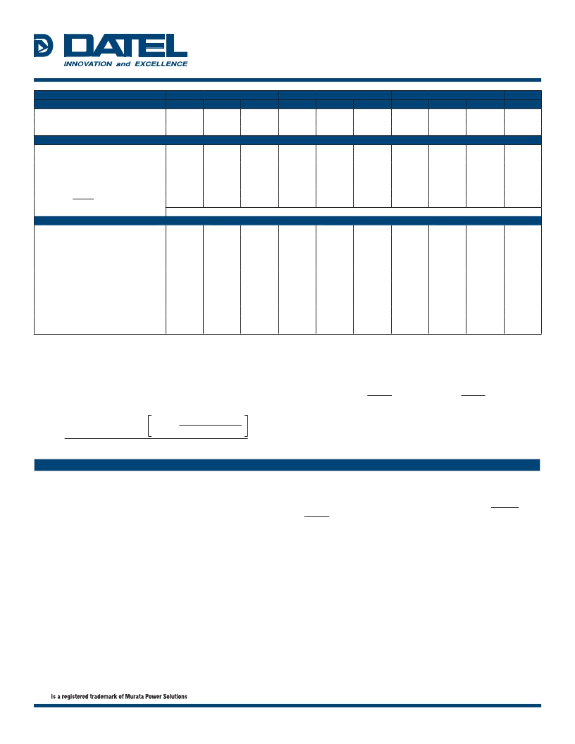
ANALOG OUTPUT
Reference Output
Reference Temperature Drift
Reference Load Current
DIGITAL OUTPUTS
Logic Levels
Logic "1"
Logic "0"
Logic Loading "1"
Logic Loading "0"
Delay, Rising Edge of Start Convert to Output Data Valid
Delay, Edge of ENABLE to Output Data Valid/Invalid
Output Coding
POWER REQUIREMENTS
Power Supply Ranges
+15V Supply
–15V Supply
+5V Supply
–5.2V Supply
Power Supply Currents
+15V Supply
–15V Supply
+5V Supply
–5.2V Supply
Power Dissipation
Power Supply Rejection
MIN.
+9.95
—
—
MAX.
+10.05
—
2.0
MIN.
+9.95
—
—
MAX.
+10.05
—
2.0
MIN.
+9.95
—
—
MAX.
+10.05
—
2.0
UNITS
Volts
ppm/°C
mA
+2.7
—
—
—
—
—
—
—
—
—
—
—
—
+0.5
–0.4
–8
35
18
+2.7
—
—
—
—
—
—
—
—
—
—
—
—
+0.5
–0.4
–8
35
18
+2.7
—
—
—
—
—
—
—
—
—
—
—
—
+0.5
–0.4
–8
35
18
Volts
Volts
mA
mA
ns
ns
Complementary Offset Binary
+14.25
–14.25
+4.75
–4.95
+15.0
–15.0
+5.0
–5.2
+15.75
–15.75
+5.25
–5.45
+14.25
–14.25
+4.75
–4.95
+15.0
–15.0
+5.0
–5.2
+15.75
–15.75
+5.25
–5.45
+14.25
–14.25
+4.9
–5.1
+15.0
–15.0
+5.0
–5.2
+15.75
–15.75
+5.25
–5.45
Volts
Volts
Volts
Volts
—
—
—
—
—
—
+35
–10
+290
–350
4.0
—
+45
–20
+320
–390
4.3
±0.04
—
—
—
—
—
—
+35
–10
+290
–350
4.0
—
+45
–20
+320
–390
4.3
±0.04
—
—
—
—
—
—
+35
–10
+290
–350
4.0
—
+45
–20
+320
–390
4.3
±0.04
mA
mA
mA
mA
Watts
%FSR/%V
ADS-945
14-Bit, 10MHz Sampling A/D Converters
DATEL
11 Cabot Boulevard, Mansfield, MA 02048-1151 USA Tel: (508) 339-3000 www.datel.com e-mail: help@datel.com
01 Apr 2011 MDA_ADS-945.B02
Page 3 of 8
相關(guān)PDF資料 |
PDF描述 |
|---|---|
| ADS-951MC | |
| ADS-CCD1202MM | |
| ADSD-1402S-EX | 2-CH 14-BIT PROPRIETARY METHOD ADC, PARALLEL ACCESS, PDSO40 |
| ADSD-1410S-EX | 2-CH 14-BIT PROPRIETARY METHOD ADC, PARALLEL ACCESS, DSO40 |
| ADSP-21020BG-120 | 32/40-Bit IEEE Floating-Point DSP Microprocessor |
相關(guān)代理商/技術(shù)參數(shù) |
參數(shù)描述 |
|---|---|
| ADS-945EX | 制造商:Murata Power Solutions 功能描述:ADC Dual 2-Step Flash 10Msps 14-bit Parallel 76-Pin |
| ADS-946 | 制造商:未知廠家 制造商全稱:未知廠家 功能描述:ADS-946 14-Bit, 8MHz Sampling A/D Converters |
| ADS-946/883 | 制造商:MURATA-PS 制造商全稱:Murata Power Solutions Inc. 功能描述:14-Bit, 8MHz Sampling A/D Converters |
| ADS-946G/883 | 制造商:Murata Power Solutions 功能描述:ADC Single 2-Step Flash 8Msps 14-bit Parallel 24-Pin SMT |
| ADS-946GC | 制造商:Murata Power Solutions 功能描述:ADC Single 2-Step Flash 8Msps 14-bit Parallel 24-Pin SMT |
發(fā)布緊急采購,3分鐘左右您將得到回復。