- 您現(xiàn)在的位置:買賣IC網(wǎng) > PDF目錄374016 > ADN2811ACP-CML-RL (ANALOG DEVICES INC) OC-48/OC-48 FEC Clock and Data Recovery IC with Integrated Limiting Amp PDF資料下載
參數(shù)資料
| 型號(hào): | ADN2811ACP-CML-RL |
| 廠商: | ANALOG DEVICES INC |
| 元件分類: | 數(shù)字傳輸電路 |
| 英文描述: | OC-48/OC-48 FEC Clock and Data Recovery IC with Integrated Limiting Amp |
| 中文描述: | CLOCK RECOVERY CIRCUIT, QCC48 |
| 封裝: | 7 X 7 MM, LEAD FREE, MO-220-VKKD-2, LFCSP-48 |
| 文件頁數(shù): | 14/16頁 |
| 文件大小: | 359K |
| 代理商: | ADN2811ACP-CML-RL |
–14–
REV. A
ADN2811
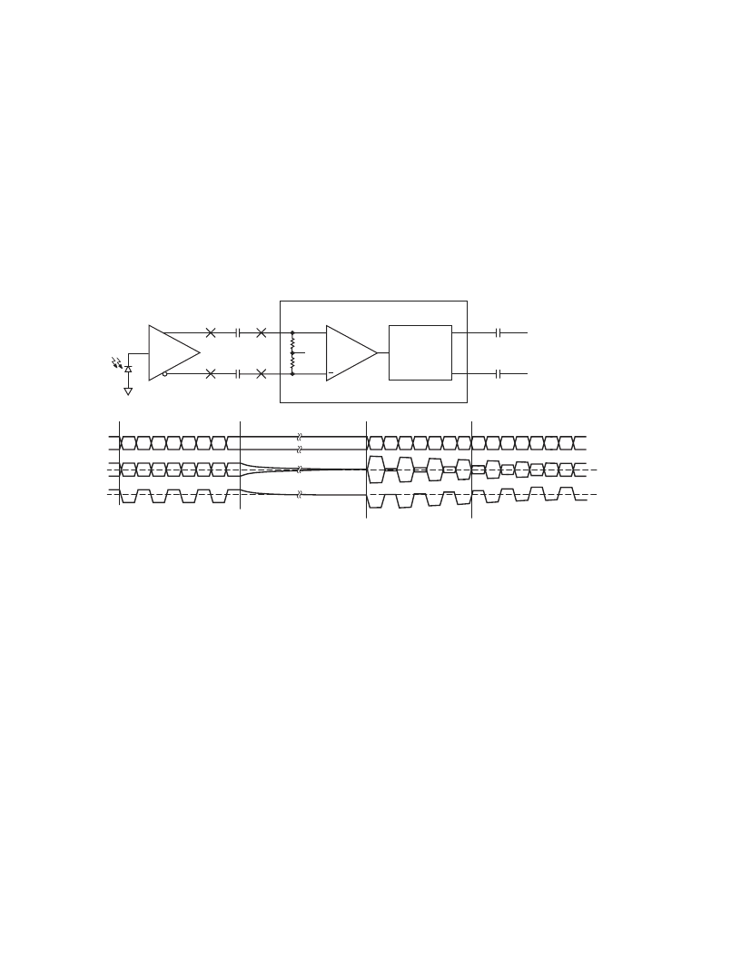
Choosing AC-Coupling Capacitors
The choice of ac-coupling capacitors at the input (PIN, NIN)
and output (DATAOUTP, DATAOUTN) of the ADN2811
must be chosen carefully. When choosing the capacitors, the
time constant formed with the two 50
resistors in the signal
path must be considered. When a large number of consecutive
identical digits (CIDs) are applied, the capacitor voltage can
drop due to baseline wander (see Figure 20), causing pattern
dependent jitter (PDJ).
For the ADN2811 to work robustly at OC-48, a minimum
capacitor of 0.1
μ
F to PIN/NIN and 0.1
μ
F on DATAOUTP/
DATAOUTN should be used. This is based on the assumption
that 1000 CIDs must be tolerated and that the PDJ should be
limited to 0.01 UI p-p.
50
ADN2811
NIN
PIN
50
V
REF
C
IN
C
IN
V2
V1
V2b
V1b
TIA
LIMAMP
CDR
C
OUT
C
OUT
DATAOUTP
DATAOUTN
+
4
3
2
1
V1
V1b
V2
V2b
V
DIFF
V
= V2–V2b
VTH = ADN2811 QUANTIZER THRESHOLD
V
REF
VTH
NOTES
1. DURING DATA PATERNS WITH HIGH TRANSITION DENSITY, DIFFERENTIAL DC VOLTAGE AT V1 AND V2 IS ZERO.
2. WHEN THE OUTPUT OF THE TIA GOES TO CID, V1 AND V1b ARE DRIVEN TO DIFFERENT DC LEVELS. V2 AND V2b DISCHARGE TO THE V
REF
LEVEL, WHICH
EFFECTIVELY INTRODUCES A DIFFERENTIAL DC OFFSET ACROSS THE AC-COUPLING CAPACITORS.
3. WHEN THE BURST OF DATA STARTS AGAIN, THE DIFFERENTIAL DC OFFSET ACROSS THE AC-COUPLING CAPACITORS IS APPLIED TO THE INPUT LEVELS,
CAUSING A DC SHIFT IN THE DIFFERENTIAL INPUT. THIS SHIFT IS LARGE ENOUGH SUCH THAT ONE OF THE STATES, EITHER HIGH OR LOW DEPENDING ON
THE LEVELS OF V1 AND V1b WHEN THE TIA WENT TO CID, IS CANCELLED OUT. THE QUANTIZER WILL NOT RECOGNIZE THIS AS A VALID STATE.
4. THE DC OFFSET SLOWLY DISCHARGES UNTIL THE DIFFERENTIAL INPUT VOLTAGE EXCEEDS THE SENSITIVITY OF THE ADN2811. THE QUANTIZER WILL BE
ABLE TO RECOGNIZE BOTH HIGH AND LOW STATES AT THIS POINT.
Figure 20. Example of Baseline Wander
DC-Coupled Application
The inputs to the ADN2811 can also be dc-coupled. This may
be necessary in burst mode applications where there are long
periods of CIDs and baseline wander cannot be tolerated. If the
inputs to the ADN2811 are dc-coupled, care must be taken not
to violate the input range and common-mode level requirements
of the ADN2811 (see Figures 21–23). If dc-coupling is required,
and the output levels of the TIA do not adhere to the levels
shown in Figures 22 and 23, then there will need to be level
shifting and/or an attenuator between the TIA outputs and the
ADN2811 inputs.
相關(guān)PDF資料 |
PDF描述 |
|---|---|
| ADN2812 | Continuous Rate 12.3 Mb/s to 2.7 Gb/s Clock and Data Recovery IC with Integrated Limiting Amp |
| ADN2812ACP | Continuous Rate 12.3 Mb/s to 2.7 Gb/s Clock and Data Recovery IC with Integrated Limiting Amp |
| ADN2812ACP-RL | Continuous Rate 12.3 Mb/s to 2.7 Gb/s Clock and Data Recovery IC with Integrated Limiting Amp |
| ADN2812ACP-RL7 | Continuous Rate 12.3 Mb/s to 2.7 Gb/s Clock and Data Recovery IC with Integrated Limiting Amp |
| ADN2819 | Multirate to 2.7 Gb/s Clock and Data Recovery IC with Integrated Limiting Amp |
相關(guān)代理商/技術(shù)參數(shù) |
參數(shù)描述 |
|---|---|
| ADN2811ACPZ-CML | 功能描述:IC CLK/DATA REC W/AMP 48-LFCSP RoHS:是 類別:集成電路 (IC) >> 時(shí)鐘/計(jì)時(shí) - 專用 系列:- 標(biāo)準(zhǔn)包裝:28 系列:- 類型:時(shí)鐘/頻率發(fā)生器 PLL:是 主要目的:Intel CPU 服務(wù)器 輸入:時(shí)鐘 輸出:LVCMOS 電路數(shù):1 比率 - 輸入:輸出:3:22 差分 - 輸入:輸出:無/是 頻率 - 最大:400MHz 電源電壓:3.135 V ~ 3.465 V 工作溫度:0°C ~ 85°C 安裝類型:表面貼裝 封裝/外殼:64-TFSOP (0.240",6.10mm 寬) 供應(yīng)商設(shè)備封裝:64-TSSOP 包裝:管件 |
| ADN2811ACPZ-CML-RL | 功能描述:IC CLK DATA REC SDH 2.66GHZ 制造商:analog devices inc. 系列:- 包裝:帶卷(TR) 零件狀態(tài):上次購買時(shí)間 PLL:是 主要用途:SONET/SDH,STM 輸入:CML 輸出:CML 電路數(shù):1 比率 - 輸入:輸出:1:2 差分 - 輸入:輸出:是/是 頻率 - 最大值:2.66GHz 電壓 - 電源:3 V ~ 3.6 V 工作溫度:-40°C ~ 85°C 安裝類型:表面貼裝 封裝/外殼:48-WFQFN 裸露焊盤 供應(yīng)商器件封裝:48-LFCSP(7x7) 標(biāo)準(zhǔn)包裝:1 |
| ADN2812 | 制造商:AD 制造商全稱:Analog Devices 功能描述:Continuous Rate 12.3 Mb/s to 2.7 Gb/s Clock and Data Recovery IC with Integrated Limiting Amp |
| ADN2812ACP | 制造商:Analog Devices 功能描述:IC CLOCK/DATA RECOVERY |
| ADN2812ACP-RL | 制造商:Analog Devices 功能描述:Clock and Data Recovery 32-Pin LFCSP EP T/R |
發(fā)布緊急采購,3分鐘左右您將得到回復(fù)。