- 您現(xiàn)在的位置:買賣IC網(wǎng) > PDF目錄373994 > ADL5390 (Analog Devices, Inc.) RF/IF Vector Multiplier PDF資料下載
參數(shù)資料
| 型號: | ADL5390 |
| 廠商: | Analog Devices, Inc. |
| 英文描述: | RF/IF Vector Multiplier |
| 中文描述: | 射頻中頻向量乘法器/ |
| 文件頁數(shù): | 14/24頁 |
| 文件大?。?/td> | 716K |
| 代理商: | ADL5390 |
ADL5390
The 3 dB bandwidth is set by choosing C
FLT
according to the
following equation:
Rev. 0 | Page 14 of 24
pF
0.5
nF
10
kHz
45
C
dB
3
+
×
≈
external
f
This equation has been verified for values of C
FLT
from 10 pF to
0.1 μF (bandwidth settings of approximately 4.5 kHz to 43 MHz).
INTERFACING TO HIGH SPEED DACs
The AD977x family of dual DACs is well suited to driving the I
and Q gain controls of the ADL5390 with fast modulating sig-
nals. While these inputs can in general be driven by any DAC,
the differential outputs and bias level of the ADI TxDAC fam-
ily allows for a direct connection between DAC and modulator.
The AD977x family of dual DACs has differential current out-
puts. The full-scale current is user programmable and is usually
set to 20 mA, that is each output swings from 0 mA to 20 mA.
The basic interface between the AD9777 DAC outputs and the
ADL5390 I and Q gain control inputs is shown in Figure 32.
Resistors R1 and R2 (R1 = R2) set the dc bias level according to
the following equation:
Bias Level
=
Average Output Current
×
R1
For example, if the full-scale current from each output is 20 mA,
each output will have an average current of 10 mA. Therefore,
to set the bias level to the recommended 0.5 V, R1 and R2
should be set to 50 each. R1 and R2 should always be equal.
If R3 is omitted, this will result in an available swing from the
DAC of 2 V p-p differential, which is twice the maximum voltage
range required by the ADL5390. DAC resolution can be maxi-
mized by adding R3, which scales down this voltage according
to the following equation:
=
Swing
Scale
Full
(
)
(
)
+
×
+
×
R3
R2
R2
R3
R2
R1
I
MAX
1
||
2
OPTIONAL
LOW-PASS
FILTER
0
R1
R2
R3
I
OUTB2
I
OUTA2
QBBM
QBBP
I
OUTB1
I
OUTA1
IBBM
IBBP
AD9777
ADL5390
OPTIONAL
LOW-PASS
FILTER
R1
R2
R3
Figure 32. Basic AD9777-to-ADL5390 Interface
R3 (
)
0
130
50 55 60 65 70 75 80 85 90
100 105
115 120
110
125
95
D
1.15
1.13
1.08
1.05
1.10
1.00
0.97
1.02
0.95
0.92
0.88
0.85
0.90
0.77
0.75
0.72
0.80
0.82
0.70
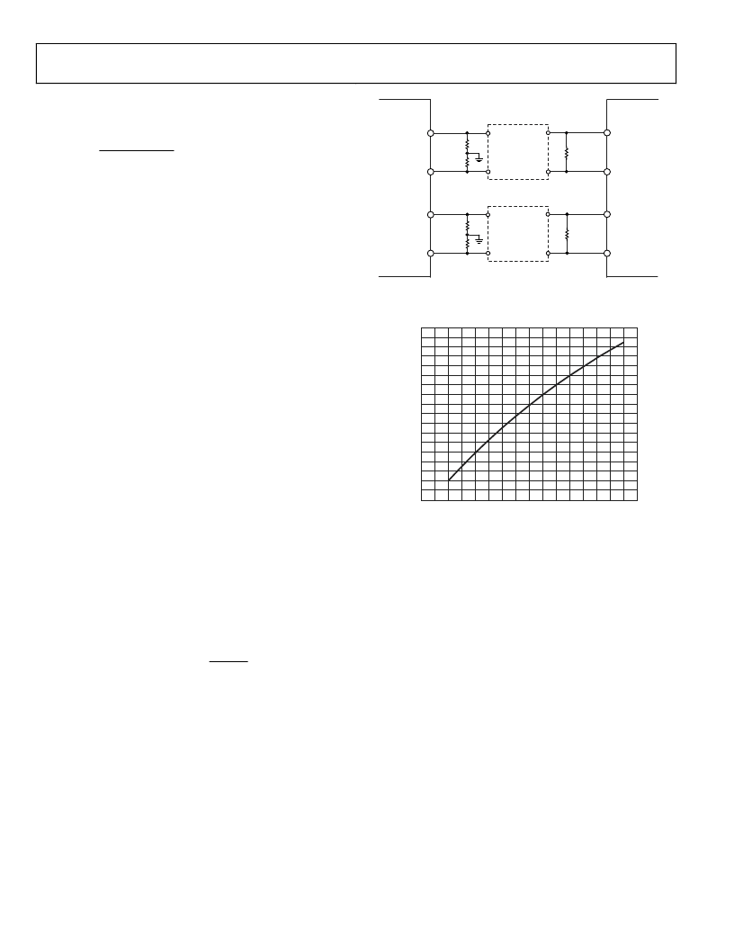
Figure 33. Peak-Peak DAC Output Swing vs.
Swing Scaling Resistor R3 (R1 = R2 = 50 )
Figure 33 shows the relationship between the value of R3 and
the peak baseband voltage with R1 and R2 equal to 50 . As
shown in Figure 33, a value of 100 for R3 will provide a
peak-peak swing of 1 V p-p differential into the ADL5390’s
I and Q inputs.
When using a DAC, low-pass image reject filters are typically
used to eliminate the Nyquist images produced by the DAC.
They also provide the added benefit of eliminating broadband
noise that might feed into the modulator from the DAC.
相關(guān)PDF資料 |
PDF描述 |
|---|---|
| ADL5391 | DC to 2.0 GHz Multiplier |
| ADL5391ACPZ-R2 | DC to 2.0 GHz Multiplier |
| ADL5391ACPZ-R7 | DC to 2.0 GHz Multiplier |
| ADL5391ACPZ-WP | DC to 2.0 GHz Multiplier |
| ADL5391-EVALZ | DC to 2.0 GHz Multiplier |
相關(guān)代理商/技術(shù)參數(shù) |
參數(shù)描述 |
|---|---|
| ADL5390ACPZ | 制造商:Analog Devices 功能描述:RF/IF VECTOR MLTPLR 24LFCSP - Tape and Reel 制造商:Analog Devices 功能描述:RF VECTOR MULTIPLIER 2.3GHZ SMD 制造商:Analog Devices 功能描述:RF Vector Multiplier,wideband,ADL5390 |
| ADL5390ACPZ-REEL7 | 功能描述:IC MULTIPLIER VECTOR 24LFCSP RoHS:是 類別:RF/IF 和 RFID >> RF 其它 IC 和模塊 系列:- 標(biāo)準(zhǔn)包裝:100 系列:* |
| ADL5390ACPZ-REEL71 | 制造商:AD 制造商全稱:Analog Devices 功能描述:RF/IF Vector Multiplier |
| ADL5390ACPZ-WP | 功能描述:IC MULTIPLIER RF VECTOR 24-LFCSP RoHS:是 類別:RF/IF 和 RFID >> RF 其它 IC 和模塊 系列:- 標(biāo)準(zhǔn)包裝:100 系列:* |
| ADL5390ACPZ-WP1 | 制造商:AD 制造商全稱:Analog Devices 功能描述:RF/IF Vector Multiplier |
發(fā)布緊急采購,3分鐘左右您將得到回復(fù)。