- 您現(xiàn)在的位置:買(mǎi)賣(mài)IC網(wǎng) > PDF目錄373986 > ADG429BN (ANALOG DEVICES INC) LC2MOS Latchable 4-/8-Channel High Performance Analog Multiplexers PDF資料下載
參數(shù)資料
| 型號(hào): | ADG429BN |
| 廠商: | ANALOG DEVICES INC |
| 元件分類: | 運(yùn)動(dòng)控制電子 |
| 英文描述: | LC2MOS Latchable 4-/8-Channel High Performance Analog Multiplexers |
| 中文描述: | 4-CHANNEL, DIFFERENTIAL MULTIPLEXER, PDIP18 |
| 封裝: | PLASTIC, DIP-18 |
| 文件頁(yè)數(shù): | 5/12頁(yè) |
| 文件大小: | 157K |
| 代理商: | ADG429BN |
REV. C
ADG428/ADG429
–5–
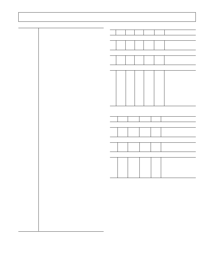
ADG428 Truth Table
A2
A1
A0
EN
WR
RS
ON SWITCH
Latching
X
X
X
X
g
1
Maintains Previous
Switch Condition
Reset
X
X
X
X
X
0
NONE
(Latches Cleared)
Transparent Operation
X
0
0
0
0
1
1
1
1
X
0
0
1
1
0
0
1
1
X
0
1
0
1
0
1
0
1
0
1
1
1
1
1
1
1
1
0
0
0
0
0
0
0
0
0
1
1
1
1
1
1
1
1
1
NONE
1
2
3
4
5
6
7
8
ADG429 Truth Table
A1
A0
EN
WR
RS
ON SWITCH PAIR
Latching
X
X
X
g
1
Maintains Previous
Switch Condition
Reset
X
X
X
X
0
NONE
(Latches Cleared)
Transparent Operation
X
0
0
1
1
X
0
1
0
1
0
1
1
1
1
0
0
0
0
0
1
1
1
1
1
NONE
1
2
3
4
TERMINOLOGY
V
DD
V
SS
Most positive power supply potential.
Most negative power supply potential in dual
supplies. In single supply applications, it may
be connected to ground.
Ground (0 V) reference.
Ohmic resistance between D and S.
Difference between the R
ON
of any two
channels.
Source leakage current when the switch is off.
Drain leakage current when the switch is off.
Channel leakage current when the switch is
on.
Analog voltage on terminals D, S.
Channel input capacitance for “OFF”
condition.
Channel output capacitance for “OFF”
condition.
“ON” switch capacitance.
Digital input capacitance.
Delay time between the 50% and 90% points
of the digital input and switch “ON”
condition.
Delay time between the 50% and 90% points
of the digital input and switch “OFF”
condition.
Delay time between the 50% and 90% points
of the digital inputs and the switch “ON”
condition when switching from one address
state to another.
“OFF” time measured between 80% points of
both switches when switching from one
address state to another.
Maximum input voltage for Logic “0.”
Minimum input voltage for Logic “1.”
Input current of the digital input.
A measure of unwanted signal which is
coupled through from one channel to another
as a result of parasitic capacitance.
A measure of unwanted signal coupling
through an “OFF” channel.
A measure of the glitch impulse transferred
from the digital input to the analog output
during switching.
Positive supply current.
Negative supply current.
GND
R
ON
R
ON
I
S
(OFF)
I
D
(OFF)
I
D
, I
S
(ON)
V
D
(V
S
)
C
S
(OFF)
C
D
(OFF)
C
D
, C
S
(ON)
C
IN
t
ON
(EN)
t
OFF
(EN)
t
TRANSITlON
t
OPEN
V
INL
V
INH
I
INL
(I
INH
)
Crosstalk
Off Isolation
Charge
Injection
I
DD
I
SS
相關(guān)PDF資料 |
PDF描述 |
|---|---|
| ADG429BP | LC2MOS Latchable 4-/8-Channel High Performance Analog Multiplexers |
| ADG429TQ | LC2MOS Latchable 4-/8-Channel High Performance Analog Multiplexers |
| ADG432TQ | LC2MOS Precision Quad SPST Switches |
| ADG433 | LC2MOS Precision Quad SPST Switches |
| ADG433ABR | LC2MOS Precision Quad SPST Switches |
相關(guān)代理商/技術(shù)參數(shù) |
參數(shù)描述 |
|---|---|
| ADG429BP | 制造商:AD 制造商全稱:Analog Devices 功能描述:LC2MOS Latchable 4-/8-Channel High Performance Analog Multiplexers |
| ADG429TQ | 制造商:Rochester Electronics LLC 功能描述:8/DUAL 4 CH.LATCHED MUX. - Bulk |
| ADG429TQ/883B | 制造商:未知廠家 制造商全稱:未知廠家 功能描述:4-Channel Analog Multiplexer |
| ADG431 | 制造商:AD 制造商全稱:Analog Devices 功能描述:LC2MOS Precision Quad SPST Switches |
| ADG431ABR | 制造商:Analog Devices 功能描述:IC SWITCH SPST QUAD CMOS |
發(fā)布緊急采購(gòu),3分鐘左右您將得到回復(fù)。