- 您現(xiàn)在的位置:買賣IC網(wǎng) > PDF目錄375254 > ADE7761ARS-REF (ANALOG DEVICES INC) Energy Metering IC with On-Chip Fault and Missing Neutral Detection PDF資料下載
參數(shù)資料
| 型號: | ADE7761ARS-REF |
| 廠商: | ANALOG DEVICES INC |
| 元件分類: | 模擬信號調(diào)理 |
| 英文描述: | Energy Metering IC with On-Chip Fault and Missing Neutral Detection |
| 中文描述: | SPECIALTY ANALOG CIRCUIT, PDSO20 |
| 封裝: | MO-150AE, SSOP-20 |
| 文件頁數(shù): | 13/28頁 |
| 文件大?。?/td> | 302K |
| 代理商: | ADE7761ARS-REF |
第1頁第2頁第3頁第4頁第5頁第6頁第7頁第8頁第9頁第10頁第11頁第12頁當(dāng)前第13頁第14頁第15頁第16頁第17頁第18頁第19頁第20頁第21頁第22頁第23頁第24頁第25頁第26頁第27頁第28頁
ADE7761
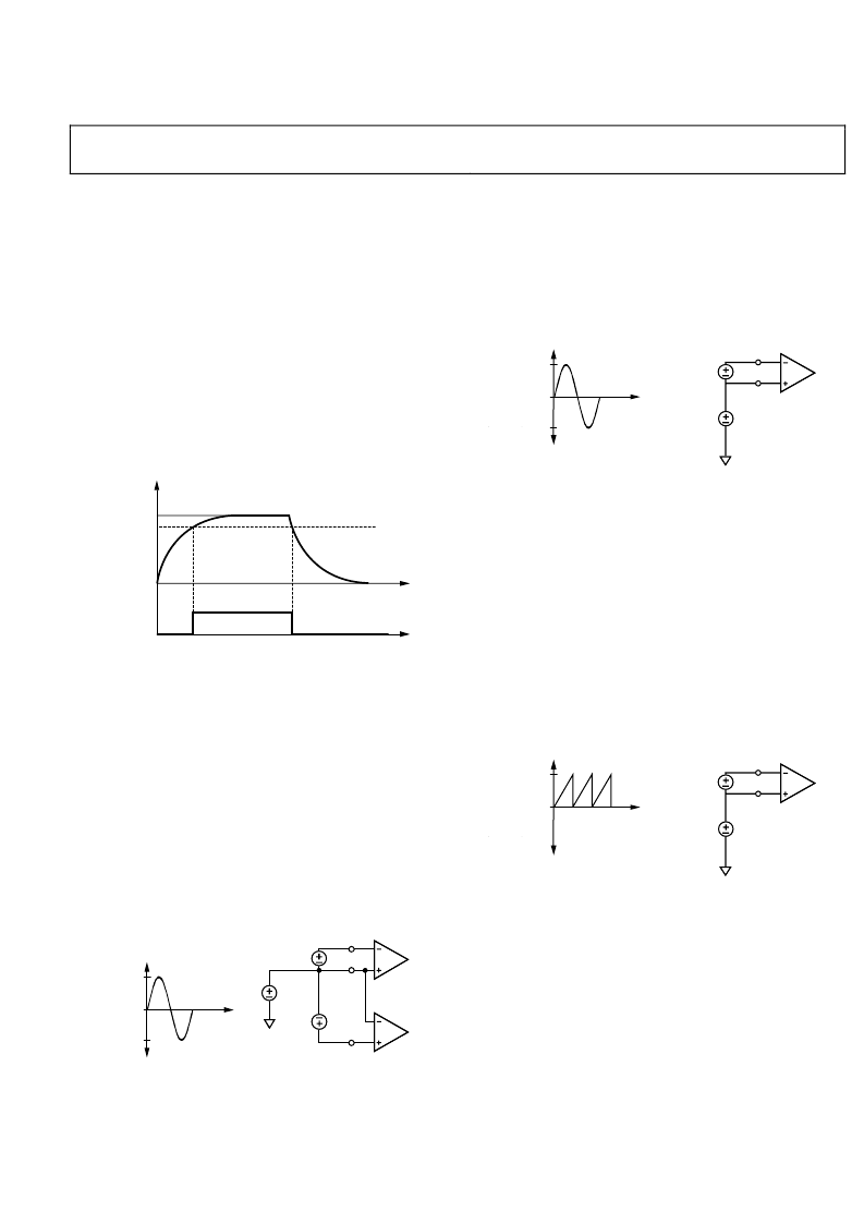
OPERATION
POWER SUPPLY MONITOR
The ADE7761 contains an on-chip power supply monitor. The
power supply (V
DD
) is continuously monitored by the ADE7761.
If the supply is less than 4 V ± 5%, the ADE7761 goes into an
inactive state, that is, no energy is accumulated and the CF, F1,
and F2 outputs are disabled. This is useful to ensure correct
device operation at power-up and during power-down. The
power supply monitor has built-in hysteresis and filtering. This
gives a high degree of immunity to false triggering due to noisy
supplies.
Rev. A | Page 13 of 28
The power supply and decoupling for the part should be such
that the ripple at V
DD
does not exceed 5 V ± 5% as specified for
normal operation.
ADE7761
REVP - FAULT - CF -
F1 - F2 OUTPUTS
INACTIVE
ACTIVE
TIME
INACTIVE
V
DD
5V
4V
0V
0
Figure 9. On-Chip Power Supply Monitoring
ANALOG INPUTS
Channel V1 (Current Channel)
The voltage outputs from the current transducers are connected
to the ADE7761 here. Channel V1 has two voltage inputs, V
1A
and V
1B
. These inputs are fully differential with respect to V
1N
.
However, at any one time, only one is selected to perform the
power calculation (see the Fault Detection section).
The maximum peak differential signal on V
1A
–V
1N
and V
1B
–V
1N
is ±660 mV.
Figure 10 shows the maximum signal levels on V
1A
, V
1B
, and V
1N
.
The differential voltage signal on the inputs must be referenced
to a common mode (usually AGND).
V
CM
+660mV + V
CM
–660mV + V
CM
DIFFERENTIAL INPUT B
±660mV MAX PEAK
V
1B
V
1N
V
1A
V1
V1
V
CM
COMMON MODE
±100mV MAX
DIFFERENTIAL INPUT A
±660mV MAX PEAK
AGND
V
1A
, V
1B
0
Figure 10. Maximum Signal Levels, Channel 1
Channel V2 (Voltage Channel)
The output of the line voltage transducer is connected to the
ADE7761 at this analog input. Channel V2 is a single-ended
voltage input. The maximum peak differential signal on
Channel 2 is ±660 mV with respect to V
2N
. Figure 11 shows the
maximum signal levels that can be connected to Channel 2.
0
V
CM
+660mV + V
CM
–660mV + V
CM
COMMON MODE
±100mV MAX
V
2N
V
2P
V
CM
V2
DIFFERENTIAL INPUT
±660mV MAX PEAK
V2
Figure 11. Maximum Signal Levels, Channel 2
The differential voltage V
2P
–V
2N
must be referenced to a
common mode (usually AGND). The analog inputs of the
ADE7761 can be driven with common-mode voltages of up to
100 mV with respect to AGND. However, the best results are
achieved using a common mode equal to AGND.
MISCAL Input
The input for the power calibration in missing neutral mode is
connected to the ADE7761 at this analog input. MISCAL is a
single-ended voltage input. It is recommended to use a dc signal
derived from the voltage reference to drive this pin. The maxi-
mum peak differential signal on MISCAL is +660 mV with
respect to V
2N
. Figure 12 shows the maximum signal levels that
can be connected to the MISCAL pin.
0
V
CM
+660mV + V
CM
COMMON MODE
±100mV MAX
V
2N
MISCAL
V
CM
MISCAL
DIFFERENTIAL INPUT
±660mV MAX PEAK
MISCAL
AGND
Figure 12. Maximum Signal Levels, MISCAL
The differential voltage MISCAL–V
2N
must be referenced to a
common mode (usually AGND). The analog inputs of the
ADE7761 can be driven with common-mode voltages of up to
100 mV with respect to AGND. However, best results are
achieved using a common mode equal to AGND.
Typical Connection Diagrams
Figure 13 shows a typical connection diagram for Channel V1.
The analog inputs are being used to monitor both the phase
and neutral currents. Because of the large potential difference
between the phase and neutral, two current transformers (CTs)
must be used to provide the isolation. Note that both CTs are
referenced to analog ground (AGND); the common-mode
相關(guān)PDF資料 |
PDF描述 |
|---|---|
| ADE7761ARSRL | Energy Metering IC with On-Chip Fault and Missing Neutral Detection |
| ADE7769 | Energy Metering IC with Integrated Oscillator and No-Load Indication |
| ADE7769AR | Energy Metering IC with Integrated Oscillator and No-Load Indication |
| ADE7769AR-REF | Energy Metering IC with Integrated Oscillator and No-Load Indication |
| ADE7769AR-RL | Energy Metering IC with Integrated Oscillator and No-Load Indication |
相關(guān)代理商/技術(shù)參數(shù) |
參數(shù)描述 |
|---|---|
| ADE7761ARSRL | 制造商:AD 制造商全稱:Analog Devices 功能描述:Energy Metering IC with On-Chip Fault and Missing Neutral Detection |
| ADE7761B | 制造商:AD 制造商全稱:Analog Devices 功能描述:Energy Metering IC with On-Chip Fault and Missing Neutral Detection |
| ADE7761BARS | 制造商:Rochester Electronics LLC 功能描述: 制造商:Analog Devices 功能描述: |
| ADE7761BARS-REF | 制造商:AD 制造商全稱:Analog Devices 功能描述:Energy Metering IC with On-Chip Fault and Missing Neutral Detection |
| ADE7761BARS-RL | 制造商:AD 制造商全稱:Analog Devices 功能描述:Energy Metering IC with On-Chip Fault and Missing Neutral Detection |
發(fā)布緊急采購,3分鐘左右您將得到回復(fù)。