- 您現(xiàn)在的位置:買賣IC網(wǎng) > PDF目錄373980 > ADE7759ARSRL (ANALOG DEVICES INC) Active Energy Metering IC with di/dt Sensor Interface PDF資料下載
參數(shù)資料
| 型號: | ADE7759ARSRL |
| 廠商: | ANALOG DEVICES INC |
| 元件分類: | 模擬信號調理 |
| 英文描述: | Active Energy Metering IC with di/dt Sensor Interface |
| 中文描述: | SPECIALTY ANALOG CIRCUIT, PDSO20 |
| 封裝: | SSOP-20 |
| 文件頁數(shù): | 18/32頁 |
| 文件大?。?/td> | 530K |
| 代理商: | ADE7759ARSRL |
第1頁第2頁第3頁第4頁第5頁第6頁第7頁第8頁第9頁第10頁第11頁第12頁第13頁第14頁第15頁第16頁第17頁當前第18頁第19頁第20頁第21頁第22頁第23頁第24頁第25頁第26頁第27頁第28頁第29頁第30頁第31頁第32頁
REV. 0
ADE7759
–18–
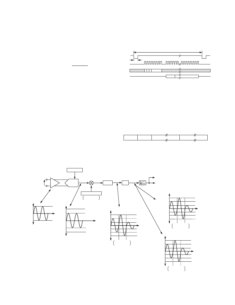
Channel 1 ADC Gain Adjust
The ADC gain in Channel 1 can be adjusted by using the multiplier
and Active Power Gain register (APGAIN[11:0]). The gain of the
ADC is adjusted by writing a two’s complement 12-bit word to
the Active Power Gain register. Below is the expression that
shows how the gain adjustment is related to the contents of the
Active Power Gain register.
Code
ADC
APGAIN
2
12
=
×
+
1
For example, when 7FFh is written to the Active Power Gain
register the ADC output is scaled up by 50%. 7FFh = 2047
decimal, 2047/2
12
= 0.5. Similarly, 801h = 2047 decimal
(signed two’s complement) and ADC output is scaled by –50%.
These two examples are graphically illustrated in Figure 23.
Channel 1 Sampling
The waveform samples may also be routed to the WAVEFORM
register (MODE[14:13] = 1, 0) to be read by the system master
(MCU). In waveform sampling mode the WSMP bit (Bit 3) in
the Interrupt Enable register must also be set to Logic 1. The
Active Power and Energy calculation will remain uninterrupted
during waveform sampling.
When in waveform sample mode, one of four output sample
rates may be chosen by using bits 11 and 12 of the Mode regis-
ter (WAVSEL1, 0). The output sample rate may be 27.9 kSPS,
14 kSPS, 7 kSPS, or 3.5 kSPS—see Mode Register section. The
interrupt request output
IRQ
signals a new sample availability
by going active low. The timing is shown in Figure 24. The 20-bit
waveform samples are transferred from the ADE7759 one byte
(eight-bits) at a time, with the most significant byte shifted out first.
The 20-bit data word is right justified and sign extended to 24
bits (three bytes)—see
Serial Interface section.
READ FROM WAVEFORM
0
0 0 01 HEX
SIGN
CHANNEL 1 DATA
–
20 BITS
SAMPLING RATE (27.9kSPS, 14kSPS, 7kSPS, OR 3.5kSPS)
16 s
IRQ
SCLK
DIN
DOUT
Figure 24. Waveform Sampling Channel 1
CHANNEL 1 AND CHANNEL 2 WAVEFORM SAMPLING
MODE
In Channel 1 and Channel 2 waveform sampling mode
(MODE[14:13] = 01), the output is a 40-bit waveform sample
data that contains both the waveform samples from Channel 1
and Channel 2 ADCs. Figure 25 shows the format of the 40-bit
waveform output.
CH2[19:16] CH1[19:16]
CH1[15:0]
CH2[15:0]
1 BYTE
2 BYTES
2 BYTES
BIT 39
BIT 0
Figure 25. 40-Bit Combined Channel 1 and Channel 2
Waveform Sample Data Format
ADC 1
HPF
REFERENCE
2.42V, 1.21V, 0.6V
V1
0V
ANALOG
INPUT
RANGE
0.5V, 0.25V,
0.125V, 62.5mV,
31.3mV, 15.6mV,
00000h
40000h
C0000h
2851Fh
D7AE1h
+FS
–
FS
+63% FS
–
63% FS
ADC OUTPUT
WORD RANGE
00000h
EBD71h
2851Fh
1428Fh
+63% FS
–
63% FS
–
94.5% FS
D7AE1h
C3852h
+94.5% FS
+31.5% FS
–
31.5% FS
3C7AEh
APGAIN[11:0]
000h
7FFh
801h
CHANNEL 1 (ACTIVE POWER)
DATA RANGE
TO MULTIPLIER
TO WAVEFORM
SAMPLE REGISTER
Sinc
3
DIGITAL LPF
00000h
F0846h
1EF74h
F7BAh
+63% FS
+31.5% FS
–
63% FS
–
94.5% FS
E108Ch
D18D2h
+94.5% FS
–
31.5% FS
2E72Eh
APGAIN[11:0]
000h
7FFh
801h
CHANNEL 1 (ACTIVE POWER)
DATA RANGE AFTER
INTEGRATOR (50Hz)
DIGITAL
INTEGRATOR
*
∫
00000h
F3190h
19CE0h
0CE70h
+63%
FS
+31.5%
FS
–
63%
FS
–
94.5%
FS
E6320h
D94B0h
+94.5%
FS
–
31.5%
FS
26B50h
APGAIN[11:0]
000h
7FFh
801h
CHANNEL 1 (ACTIVE POWER)
DATA RANGE AFTER
INTEGRATOR (60Hz)
50Hz
60Hz
V1P
V1N
PGA1
V1
MULTIPLIER
{GAIN[4:3]}
{GAIN[2:0]}
1, 2, 4,
8, 16
801HEX
–
7FFHEX
APGAIN[11:0]
*
WHEN DIGITAL INTEGRATOR IS ENABLED, FULL-SCALE OUTPUT DATA VARIES DEPENDING
ON THE SIGNAL FREQUENCY BECAUSE OF
–
20dB/DECADE FREQUENCY RESPONSE.
Figure 23. ADC and Signal Processing in Channel 1
相關PDF資料 |
PDF描述 |
|---|---|
| ADE7759ARS | 8-Channel 14-Bit Single-Supply Voltage-Output DAC; Package: LQFP (10x10mm); No of Pins: 52; Temperature Range: Industrial |
| ADE7759 | Active Energy Metering IC with di/dt Sensor Interface |
| ADE7760ARSRL | Energy Metering IC with On-Chip Fault Detection |
| ADE7760 | 8-Channel 14-Bit Single-Supply Voltage-Output DAC; Package: LQFP (10x10mm); No of Pins: 52; Temperature Range: Industrial |
| ADE7760ARS | Energy Metering IC with On-Chip Fault Detection |
相關代理商/技術參數(shù) |
參數(shù)描述 |
|---|---|
| ADE7759ARSZ | 功能描述:IC ENERGY METERING 1PHASE 20SSOP RoHS:是 類別:集成電路 (IC) >> PMIC - 能量測量 系列:- 產品培訓模塊:Lead (SnPb) Finish for COTS Obsolescence Mitigation Program 標準包裝:2,500 系列:* |
| ADE7759ARSZRL | 功能描述:IC ENERGY METERING 1PHASE 20SSOP RoHS:是 類別:集成電路 (IC) >> PMIC - 能量測量 系列:- 產品培訓模塊:Lead (SnPb) Finish for COTS Obsolescence Mitigation Program 標準包裝:2,500 系列:* |
| ADE7760 | 制造商:AD 制造商全稱:Analog Devices 功能描述:Energy Metering IC with On-Chip Fault Detection |
| ADE7760ARS | 制造商:Analog Devices 功能描述:Energy Measurement 20-Pin SSOP 制造商:Analog Devices 功能描述:ENERGY METER IC W/ ONCHIP FAULT & OSCIL. - Rail/Tube |
| ADE7760ARSRL | 制造商:Analog Devices 功能描述:Energy Measurement 20-Pin SSOP T/R 制造商:Analog Devices 功能描述:ENERGY METER IC W/ONCHIP FAULT & OSCIL. - Tape and Reel |
發(fā)布緊急采購,3分鐘左右您將得到回復。