- 您現(xiàn)在的位置:買賣IC網(wǎng) > PDF目錄373980 > ADE7758 (Analog Devices, Inc.) Poly Phase Multifunction Energy Metering IC with Per Phase Information PDF資料下載
參數(shù)資料
| 型號: | ADE7758 |
| 廠商: | Analog Devices, Inc. |
| 英文描述: | Poly Phase Multifunction Energy Metering IC with Per Phase Information |
| 中文描述: | 多相多功能電能計量IC每相位信息 |
| 文件頁數(shù): | 23/68頁 |
| 文件大小: | 1584K |
| 代理商: | ADE7758 |
第1頁第2頁第3頁第4頁第5頁第6頁第7頁第8頁第9頁第10頁第11頁第12頁第13頁第14頁第15頁第16頁第17頁第18頁第19頁第20頁第21頁第22頁當前第23頁第24頁第25頁第26頁第27頁第28頁第29頁第30頁第31頁第32頁第33頁第34頁第35頁第36頁第37頁第38頁第39頁第40頁第41頁第42頁第43頁第44頁第45頁第46頁第47頁第48頁第49頁第50頁第51頁第52頁第53頁第54頁第55頁第56頁第57頁第58頁第59頁第60頁第61頁第62頁第63頁第64頁第65頁第66頁第67頁第68頁
ADE7758
Rev. A | Page 23 of 68
0
ADC
TO VOLTAGE RMS
CALCULATION AND
WAVEFORM SAMPLING
TO ACTIVE AND
REACTIVE ENERGY
CACLULATION
VAP
+
PGA
–
VN
VA
GAIN[6:5]
×
1,
2,
4
LPF OUTPUT
WORD RANGE
0xD869
0x0
0x2797
50Hz
LPF OUTPUT
WORD RANGE
0xD8B8
0x0
0x2748
60Hz
0xD7AE
0x0
0x2852
PHASE
CALIBRATION
Φ
PHCAL[6:0]
ANALOG INPUT
RANGE
VA
0V
0.5V
GAIN
LPF1
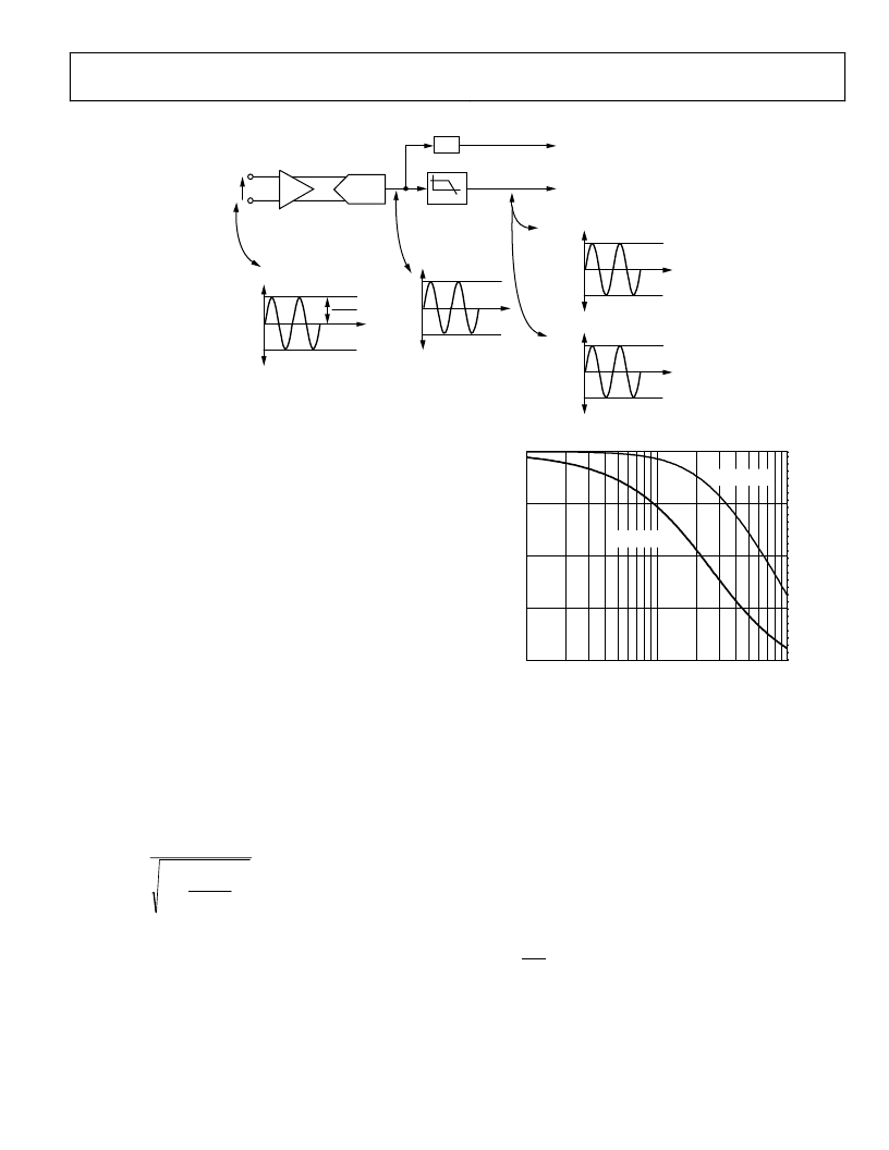
Figure 49. ADC and Signal Processing in Voltage Channel
For active and reactive energy measurements, the output of the
ADC passes directly to the multipliers and is not filtered. This
solution avoids the much larger multibit multiplier and does not
affect the accuracy of the measurement. A HPF is not imple-
mented on the voltage channel to remove the dc offset because
the HPF on the current channel alone should be sufficient to
eliminate error due to ADC offsets in the power calculation.
However, ADC offset in the voltage channels produces large
errors in the voltage rms calculation and affects the accuracy
of the apparent energy calculation.
Voltage Channel Sampling
The waveform samples on the voltage channels can also be
routed to the WFORM register. However, before passing to the
WFORM register, the ADC outputs pass through a single-pole,
low-pass filter (LPF1) with a cutoff frequency at 260 Hz.
Figure 50 shows the magnitude and phase response of LPF1.
This filter attenuates the signal slightly. For example, if the line
frequency is 60 Hz, the signal at the output of LPF1 is attenuated
by 3.575%. The waveform samples are 16-bit, twos complement
data ranging between 0x2748 (+10,056d) and 0xD8B8 (10,056d).
The data are sign extended to 24 bit in the WFORM register.
( )
f
dB
225
.
974
.
z
H
260
Hz
60
1
1
2
=
=
+
=
H
0
–20
–40
–60
–80
0
–10
–20
–30
–40
10
100
1k
0
FREQUENCY (Hz)
P
G
(60Hz; –0.2dB)
(60Hz; –13
°
)
Figure 50. Magnitude and Phase Response of LPF1
Note that LPF1 does not affect the active and reactive energy
calculation because it is used only in the waveform sampling
signal path. However, waveform samples are used for the
voltage rms calculation and the subsequent apparent energy
accumulation.
WAVSEL[2:0] bits in the WAVMODE register should be set to
001 (binary) to start voltage waveform sampling. PHSEL[1:0]
bits control the phase from which the samples are routed. When
in waveform sampling mode, one of four output sample rates
can be chosen by changing Bit 5 and Bit 6 of the WAVMODE
register (see Table 16). The available output sample rates are
26.0 kSPS, 13.5 kSPS, 6.5 kSPS, or 3.3 kSPS. By setting the WSMP
bit in the interrupt mask register to Logic 1, the interrupt request
output IRQ goes active low when a sample is available. Figure 40
shows the timing. The 24-bit waveform samples are transferred
from the ADE7758 one byte (8 bits) at a time, with the most
significant byte shifted out first. The sign of the register is
extended in the upper 8 bits. The timing is the same as that
for the current channels (see Figure 40).
相關PDF資料 |
PDF描述 |
|---|---|
| ADE7758ARW | Poly Phase Multifunction Energy Metering IC with Per Phase Information |
| ADE7758ARWRL | Poly Phase Multifunction Energy Metering IC with Per Phase Information |
| ADE7758ARWZ | Poly Phase Multifunction Energy Metering IC with Per Phase Information |
| ADE7758ARWZRL | Poly Phase Multifunction Energy Metering IC with Per Phase Information |
| ADE7759ARSRL | Active Energy Metering IC with di/dt Sensor Interface |
相關代理商/技術參數(shù) |
參數(shù)描述 |
|---|---|
| ADE7758ARW | 制造商:Analog Devices 功能描述:Energy Measurement 24-Pin SOIC W 制造商:Analog Devices 功能描述:IC ENERGY METER |
| ADE7758ARWRL | 制造商:Analog Devices 功能描述:Energy Measurement 24-Pin SOIC W T/R 制造商:Analog Devices 功能描述:IC ENERGY METER |
| ADE7758ARWZ | 功能描述:IC ENERGY METERING 3PHASE 24SOIC RoHS:是 類別:集成電路 (IC) >> PMIC - 能量測量 系列:- 產(chǎn)品培訓模塊:Lead (SnPb) Finish for COTS Obsolescence Mitigation Program 標準包裝:2,500 系列:* |
| ADE7758ARWZ | 制造商:Analog Devices 功能描述:ENERGY METERING IC 制造商:Analog Devices 功能描述:IC, POLY-PHASE ENERGY METERING, SOIC-24 |
| ADE7758ARWZ | 制造商:Analog Devices 功能描述:IC ENERGY METER 3 PHASE SOIC-24 |
發(fā)布緊急采購,3分鐘左右您將得到回復。