- 您現(xiàn)在的位置:買賣IC網(wǎng) > PDF目錄375252 > ADC803SMQ High Speed ANALOG-TO-DIGITAL CONVERTER PDF資料下載
參數(shù)資料
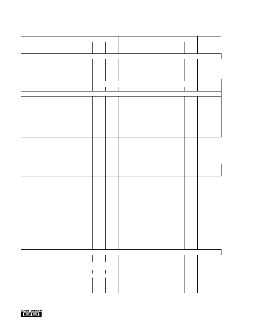
| 型號(hào): | ADC803SMQ |
| 英文描述: | High Speed ANALOG-TO-DIGITAL CONVERTER |
| 中文描述: | 高速模擬數(shù)字轉(zhuǎn)換器 |
| 文件頁數(shù): | 2/4頁 |
| 文件大?。?/td> | 44K |
| 代理商: | ADC803SMQ |
2
ADC803
SPECIFICATIONS
At +25
°
C, rated power supplies, 1.5
μ
s conversion time, and after 6-minute warm-up, unless otherwise noted.
The information provided herein is believed to be reliable; however, BURR-BROWN assumes no responsibility for inaccuracies or omissions. BURR-BROWN assumes
no responsibility for the use of this information, and all use of such information shall be entirely at the user’s own risk. Prices and specifications are subject to change
without notice. No patent rights or licenses to any of the circuits described herein are implied or granted to any third party. BURR-BROWN does not authorize or warrant
any BURR-BROWN product for use in life support devices and/or systems.
ADC803CM
ADC803BM
ADC803SM
PARAMETER
MIN
TYP
MAX
MIN
TYP
MAX
MIN
TYP
MAX
UNITS
RESOLUTION
12
12
12
Bits
INPUTS
ANALOG
Voltage Ranges: Bipolar
±
5,
±
10
0 to –10
1.4
2.4
*
*
*
*
*
*
*
*
V
V
k
k
Unipolar
Impedance: –10V to 0V,
±
5V
±
10V
DIGITAL
Convert Command
Logic Loading
4
*
*
TTL Loads
TRANSFER CHARACTERISTICS
ACCURACY
Gain Error
(1)
Offset Error
(1)
:Unipolar
±
0.04
±
0.05
±
0.02
±
0.1
±
0.2
±
0.1
±
0.08
±
0.07
*
±
0.2
±
0.3
±
0.2
±
0.04
*
*
±
0.1
*
*
%
% of FSR
(2)
% of FSR
Bipolar
Linearity Error:
1.5
μ
s Conversion Time
1.0
μ
s Conversion Time
Differential Linearity Error:
1.5
μ
s Conversion Time
1.0
μ
s Conversion Time
Inherent Quantization Error
±
0.009
±
0.015
±
0.012
±
0.020
±
0.020
±
0.012
±
0.015
% of FSR
% of FSR
±
0.020
±
0.012
±
0.015
±
0.024
±
0.020
*
*
*
*
% of FSR
% of FSR
LSB
±
0.024
*
1/2
POWER SUPPLY SENSITIVITY
Gain and Offset: +15VDC
±
0.0036
±
0.0005
±
0.001
±
0.7
None
±
0.8
*
*
*
*
*
*
*
*
*
*
*
*
% of FSR/%V
CC
% of FSR/%V
CC
% of FSR/%V
DD
%/%V
CC
%/%V
CC
%/%V
DD
–15VDC
+5VDC
Conversion Time: +15VDC
–15VDC
+5VDC
CONVERSION TIME
Factory Set
Range of Adjustments
1.3
0.8
1.5
2.2
*
*
*
*
*
*
*
*
μ
s
μ
s
DRIFT
Gain
Offset: Unipolar
Bipolar
Linearity Error
–25
°
C to +85
°
C:
1.5
μ
s Conversion Time
1.0
μ
s Conversion Time
–55
°
C to +125
°
C:
1.7
μ
s Conversion Time, max
(4)
Differential Linearity Error
–25
°
C to +85
°
C:
1.5
μ
s Conversion Time
1.0
μ
s Conversion Time
–55
°
C to +125
°
C:
1.7
μ
s Conversion Time, max
(4)
Conversion Time
No Missing Code Temp. Range:
1.5
μ
s Conversion Time
1.7
μ
s Conversion Time, max
(4)
±
10
±
2
±
3
±
30
±
7
±
10
±
15
±
3
±
5
*
*
*
*
*
*
*
*
*
ppm of FSR/
°
C
ppm of FSR/
°
C
ppm of FSR/
°
C
±
0.012
±
0.018
±
0.024
*
*
% of FSR
% of FSR
±
0.015
±
0.020
±
0.015
±
0.024
% of FSR
±
0.012
±
0.018
±
0.024
% of FSR
% of FSR
±
0.015
±
0.024
±
0.1
±
0.015
*
±
0.024
% of FSR
% of FSR
*
–25
+85
*
*
°
C
°
C
–55
+125
OUTPUT
DIGITAL DATA
Parallel
Output Codes: Unipolar Complementary Straight Binary
Bipolar
Output Drive
Status
Logic “1” During Conversion
Status Output Drive
Internal Clock
Clock Output Drive
Frequency (without external clock adj.)
*
*
*
*
Bipolar Offset Binary
6
*
*
TTL Loads
*
*
6
*
*
TTL Loads
3
*
*
TTL Loads
MHz
8
*
*
Negative pulse 50ns wide (min) trailing edge (0 to 1) initiates conversion.
相關(guān)PDF資料 |
PDF描述 |
|---|---|
| ADC87 | 12-bit, 8 Usec Military A/D Converter |
| ADC87H | 12-bit, 8 Usec Military A/D Converter |
| ADCDS-1403 | 14-Bit, 3 Megapixels/Second Imaging Signal Processor |
| ADCDS-1403EX | 14-Bit, 3 Megapixels/Second Imaging Signal Processor |
| ADCMP341ARJ | Dual Comparators with 400mV Reference and programmable Hysteresis |
相關(guān)代理商/技術(shù)參數(shù) |
參數(shù)描述 |
|---|---|
| ADC804 | 制造商:BB 制造商全稱:BB 功能描述:SERIAL OUTPUT ANALOG-TO-DIGITAL CONVERTER |
| ADC804BH | 制造商:BB 制造商全稱:BB 功能描述:SERIAL OUTPUT ANALOG-TO-DIGITAL CONVERTER |
| ADC804BH-BI | 制造商:BB 制造商全稱:BB 功能描述:SERIAL OUTPUT ANALOG-TO-DIGITAL CONVERTER |
| ADC804BHQ | 制造商:BB 制造商全稱:BB 功能描述:SERIAL OUTPUT ANALOG-TO-DIGITAL CONVERTER |
| ADC804SH | 制造商:BB 制造商全稱:BB 功能描述:SERIAL OUTPUT ANALOG-TO-DIGITAL CONVERTER |
發(fā)布緊急采購(gòu),3分鐘左右您將得到回復(fù)。