- 您現(xiàn)在的位置:買賣IC網(wǎng) > PDF目錄373974 > ADA4937-1 (Analog Devices, Inc.) Ultralow Distortion, Differential ADC Driver PDF資料下載
參數(shù)資料
| 型號(hào): | ADA4937-1 |
| 廠商: | Analog Devices, Inc. |
| 英文描述: | Ultralow Distortion, Differential ADC Driver |
| 中文描述: | 超低失真差分ADC驅(qū)動(dòng)器 |
| 文件頁(yè)數(shù): | 18/28頁(yè) |
| 文件大小: | 448K |
| 代理商: | ADA4937-1 |
第1頁(yè)第2頁(yè)第3頁(yè)第4頁(yè)第5頁(yè)第6頁(yè)第7頁(yè)第8頁(yè)第9頁(yè)第10頁(yè)第11頁(yè)第12頁(yè)第13頁(yè)第14頁(yè)第15頁(yè)第16頁(yè)第17頁(yè)當(dāng)前第18頁(yè)第19頁(yè)第20頁(yè)第21頁(yè)第22頁(yè)第23頁(yè)第24頁(yè)第25頁(yè)第26頁(yè)第27頁(yè)第28頁(yè)
ADA4937-1
THEORY OF OPERATION
The ADA4937-1 differs from conventional op amps in that it
has two outputs whose voltages move in opposite directions.
Like an op amp, it relies on open-loop gain and negative
feedback to force these outputs to the desired voltages. The
ADA4937-1 behaves much like a standard voltage feedback op
amp and makes it easier to perform single-ended-to-differential
conversions, common-mode level shifting, and amplifications
of differential signals. Also like an op amp, the ADA4937-1 has
high input impedance and low output impedance.
Two feedback loops are employed to control the differential and
common-mode output voltages. The differential feedback, set
with external resistors, controls only the differential output
voltage. The common-mode feedback controls only the common-
mode output voltage. This architecture makes it easy to set the
output common-mode level to any arbitrary value. It is forced,
by internal common-mode feedback, to be equal to the voltage
applied to the V
OCM
input, without affecting the differential
output voltage.
The ADA4937-1 architecture results in outputs that are highly
balanced over a wide frequency range without requiring tightly
matched external components. The common-mode feedback
loop forces the signal component of the output common-
mode voltage to zero. This results in nearly perfectly balanced
differential outputs that are identical in amplitude and are
exactly 180° apart in phase.
ANALYZING AN APPLICATION CIRCUIT
The ADA4937-1 uses open-loop gain and negative feedback to
force its differential and common-mode output voltages in such
a way as to minimize the differential and common-mode error
voltages. The differential error voltage is defined as the voltage
between the differential inputs labeled +IN and IN (see
Figure 46). For most purposes, this voltage can be assumed to
be zero. Similarly, the difference between the actual output
common-mode voltage and the voltage applied to V
OCM
can also
be assumed to be zero. Starting from these two assumptions,
any application circuit can be analyzed.
Rev. 0 | Page 18 of 28
SETTING THE CLOSED-LOOP GAIN
The differential-mode gain of the circuit in Figure 46 can be
determined by
G
F
dm
IN
dm
OUT
V
R
R
V
=
,
,
This assumes the input resistors (
R
G
) and feedback resistors (
R
F
)
on each side are equal.
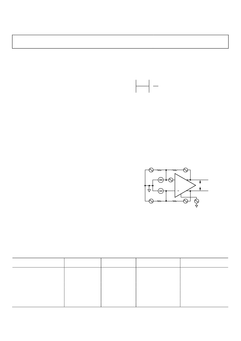
ESTIMATING THE OUTPUT NOISE VOLTAGE
The differential output noise of the ADA4937-1 can be
estimated using the noise model in Figure 47. The input-
referred noise voltage density, v
nIN
, is modeled as a differential
input, and the noise currents, i
nIN
and i
nIN+
, appear between
each input and ground. The noise currents are assumed to be
equal and produce a voltage across the parallel combination of
the gain and feedback resistances. v
nCM
is the noise voltage
density at the V
OCM
pin. Each of the four resistors contributes
(4kTR
x
)
1/2
. Table 8 summarizes the input noise sources, the
multiplication factors, and the output-referred noise density terms.
0
ADA4937-1
+
R
F2
V
nOD
V
nCM
V
OCM
V
nIN
R
F1
R
G2
R
G1
V
nRF1
V
nRF2
V
nRG1
V
nRG2
i
nIN+
i
nIN–
Figure 47. ADA4937-1 Noise Model
Table 8. Output Noise Voltage Density Calculations
Input Noise Contribution
Differential Input
Inverting Input
Noninverting Input
V
OCM
Input
Gain Resistor R
G1
Gain Resistor R
G2
Feedback Resistor R
F1
Feedback Resistor R
F2
Input Noise Term
v
nIN
i
nIN
i
nIN+
v
nCM
v
nRG1
v
nRG2
v
nRF1
v
nRF2
Input Noise
Voltage Density
v
nIN
i
nIN
× (R
G2
||R
F2
)
i
nIN+
× (R
G1
||R
F1
)
v
nCM
(4kTR
G1
)
1/2
(4kTR
G2
)
1/2
(4kTR
F1
)
1/2
(4kTR
F2
)
1/2
Output
Multiplication Factor
G
N
G
N
G
N
G
N
(β
1
β
2
)
G
N
(1 β
2
)
G
N
(1 β
1
)
1
1
Output Noise
Voltage Density Term
v
nO1
= G
N
(v
nIN
)
v
nO2
= G
N
[i
nIN
× (R
G2
||R
F2
)]
v
nO3
= G
N
[i
nIN+
× (R
G1
||R
F1
)]
v
nO4
= G
N
(β
1
β
2
)(v
nCM
)
v
nO5
= G
N
(1 β
2
)(4kTR
G1
)
1/2
v
nO6
= G
N
(1 β
1
)(4kTR
G2
)
1/2
v
nO7
= (4kTR
F1
)
1/2
v
nO8
= (4kTR
F2
)
1/2
相關(guān)PDF資料 |
PDF描述 |
|---|---|
| ADA4937-1_07 | Ultralow Distortion, Differential ADC Driver |
| ADA4937-1YCPZ-R2 | Ultralow Distortion, Differential ADC Driver |
| ADA4937-1YCPZ-R7 | Ultralow Distortion, Differential ADC Driver |
| ADA4937-1YCPZ-RL | Ultralow Distortion, Differential ADC Driver |
| ADA4938-1_07 | Ultra-Low Distortion Differential ADC Driver |
相關(guān)代理商/技術(shù)參數(shù) |
參數(shù)描述 |
|---|---|
| ADA4937-1_07 | 制造商:AD 制造商全稱:Analog Devices 功能描述:Ultralow Distortion, Differential ADC Driver |
| ADA4937-1YCP-EBZ | 功能描述:BOARD EVAL FOR ADA4937-1YCP RoHS:是 類別:編程器,開發(fā)系統(tǒng) >> 評(píng)估板 - 運(yùn)算放大器 系列:- 產(chǎn)品培訓(xùn)模塊:Lead (SnPb) Finish for COTS Obsolescence Mitigation Program 標(biāo)準(zhǔn)包裝:1 系列:- |
| ADA4937-1YCPZ-R2 | 制造商:Analog Devices 功能描述:SP Amp DIFF AMP Single 5.25V 16-Pin LFCSP EP T/R 制造商:Analog Devices 功能描述:SP AMP DIFF AMP SGL 5.25V 16LFCSP EP - Tape and Reel 制造商:Rochester Electronics LLC 功能描述:- Bulk 制造商:Analog Devices 功能描述:SP Amp DIFF AMP Single 5.25V 16-Pin LFCSP EP Tape & Reel 制造商:Analog Devices 功能描述:IC ADC DRIVERDIFF16LFCSP 制造商:Analog Devices 功能描述:OP Amp Differential ADC Driver LFCSP16 |
| ADA4937-1YCPZ-R2 | 制造商:Analog Devices 功能描述:IC DIFF AMP 1.9GHZ 6000V/S LFCSP-16 |
| ADA4937-1YCPZ-R7 | 功能描述:IC ADC DRIVER DIFF 16-LFCSP RoHS:是 類別:集成電路 (IC) >> 線性 - 放大器 - 專用 系列:- 產(chǎn)品培訓(xùn)模塊:Lead (SnPb) Finish for COTS Obsolescence Mitigation Program 標(biāo)準(zhǔn)包裝:60 系列:- 類型:可變?cè)鲆娣糯笃?應(yīng)用:CATV 安裝類型:表面貼裝 封裝/外殼:20-WQFN 裸露焊盤 供應(yīng)商設(shè)備封裝:20-TQFN-EP(5x5) 包裝:托盤 |
發(fā)布緊急采購(gòu),3分鐘左右您將得到回復(fù)。