- 您現(xiàn)在的位置:買賣IC網(wǎng) > PDF目錄373972 > AD9983AKSTZ-1701 (Analog Devices, Inc.) High Performance 8-Bit Display Interface PDF資料下載
參數(shù)資料
| 型號(hào): | AD9983AKSTZ-1701 |
| 廠商: | Analog Devices, Inc. |
| 英文描述: | High Performance 8-Bit Display Interface |
| 中文描述: | 高性能8位顯示接口 |
| 文件頁(yè)數(shù): | 20/44頁(yè) |
| 文件大小: | 470K |
| 代理商: | AD9983AKSTZ-1701 |
第1頁(yè)第2頁(yè)第3頁(yè)第4頁(yè)第5頁(yè)第6頁(yè)第7頁(yè)第8頁(yè)第9頁(yè)第10頁(yè)第11頁(yè)第12頁(yè)第13頁(yè)第14頁(yè)第15頁(yè)第16頁(yè)第17頁(yè)第18頁(yè)第19頁(yè)當(dāng)前第20頁(yè)第21頁(yè)第22頁(yè)第23頁(yè)第24頁(yè)第25頁(yè)第26頁(yè)第27頁(yè)第28頁(yè)第29頁(yè)第30頁(yè)第31頁(yè)第32頁(yè)第33頁(yè)第34頁(yè)第35頁(yè)第36頁(yè)第37頁(yè)第38頁(yè)第39頁(yè)第40頁(yè)第41頁(yè)第42頁(yè)第43頁(yè)第44頁(yè)
AD9983A
Preliminary Technical Data
Rev. PrA | Page 20 of 44
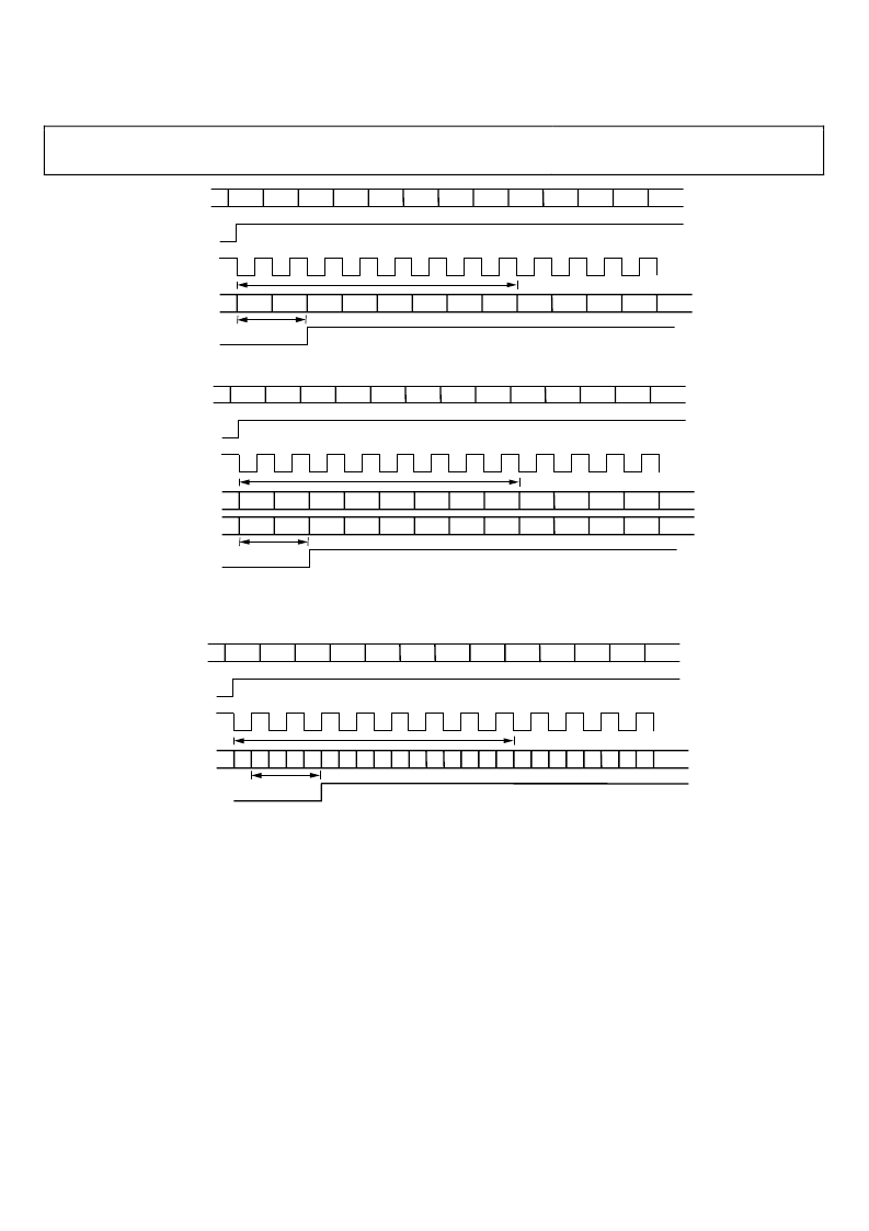
DATAIN
P0
P1
P2
P5
P3
P4
P9
P6
P8
P10
P11
P7
HSYNCx
DATACK
8 CLOCK CYCLE DELAY
DATAOUT
P0
P1
P2
P3
2 CLOCK CYCLE DELAY
HSOUT
0
Figure 15. 4:4:4 Timing Mode
DATAIN
P0
P1
P2
P5
P3
P4
P9
P6
P8
P10
P11
P7
HSYNCx
DATACK
8 CLOCK CYCLE DELAY
CB/CROUT
CB0
CR0
CB2
CR2
YOUT
Y0
Y1
Y2
Y3
2 CLOCK CYCLE DELAY
NOTES
1. PIXEL AFTER HSOUT CORRESONDS TO BLUE INPUT.
2. EVEN NUMBER OF PIXEL DELAY BETWEEN HSOUT AND DATAOUT.
Figure 16. 4:2:2 Timing Mode
HSOUT
0
DATAIN
P0
P1
P2
P5
P3
P4
P9
P6
P8
P10
P11
P7
HSYNCx
DATACK
8 CLOCK CYCLE DELAY
2 CLOCK CYCLE DELAY
DDR NOTES
1. OUTPUT DATACK MAY BE DELAYED 1/4 CLOCK PERIOD IN THE REGISTERS.
2. SEE PROJECT DOCUMENT FOR VALUES OF F (FALLING EDGE) AND R (RISING EDGE).
3. FOR DDR 4:2:2 MODE: TIMING IS IDENTICAL, VALUES OF FAND R CHANGE.
GENERAL NOTES
1. DATA DELAY MAY VARY ± ONE CLOCK CYCLE, DEPENDING ON PHASE SETTING.
2. ADCs SAMPLE INPUT ON FALLING EDGE OF DATACK.
3. HSYNC SHOWN IS ACTIVE HIGH (EDGE SHOWN IS LEADING EDGE).
HSOUT
0
F0 R0
F1 R1 F2 R2 F3 R3
Figure 17. Double Data Rate (DDR) Timing Mode
HSYNC TIMING
The Hsync is processed in the AD9983A to eliminate ambiguity
in the timing of the leading edge with respect to the phase-
delayed pixel clock and data.
The Hsync input is used as a reference to generate the pixel
sampling clock. The sampling phase can be adjusted with
respect to Hsync through a full 360° in 32 steps via the phase
adjust register (to optimize the pixel sampling time). Display
systems use Hsync to align memory and display write cycles, so
it is important to have a stable timing relationship between
Hsync output (HSOUT) and the data clock (DATACK).
Three things happen to Hsync in the AD9983A. First, the
polarity of Hsync input is determined and thus has a known
output polarity. The known output polarity can be programmed
either active high or active low (Register 0x12, Bit 3). Second,
HSOUT is aligned with DATACK and data outputs. Third, the
duration of HSOUT (in pixel clocks) is set via Register 0x13.
HSOUT is the sync signal that should be used to drive the rest
of the display system.
相關(guān)PDF資料 |
PDF描述 |
|---|---|
| AD9983A | High Performance 8-Bit Display Interface |
| AD9983AKCPZ-140 | High Performance 8-Bit Display Interface |
| AD9983AKCPZ-1401 | High Performance 8-Bit Display Interface |
| AD9983AKCPZ-170 | High Performance 8-Bit Display Interface |
| AD9983AKCPZ-1701 | High Performance 8-Bit Display Interface |
相關(guān)代理商/技術(shù)參數(shù) |
參數(shù)描述 |
|---|---|
| AD9983KSTZ-110 | 制造商:Rochester Electronics LLC 功能描述: 制造商:Analog Devices 功能描述: |
| AD9983KSTZ-140 | 制造商:Rochester Electronics LLC 功能描述: 制造商:Analog Devices 功能描述: |
| AD9983KSTZ-170 | 制造商:Rochester Electronics LLC 功能描述:- Bulk 制造商:Analog Devices 功能描述: |
| AD9984A | 制造商:AD 制造商全稱:Analog Devices 功能描述:High Performance 10-Bit Display Interface |
| AD9984A/PCB | 制造商:Analog Devices 功能描述:DISPLAY INTRFC - Bulk |
發(fā)布緊急采購(gòu),3分鐘左右您將得到回復(fù)。