- 您現(xiàn)在的位置:買賣IC網(wǎng) > PDF目錄373969 > AD9870EB (Analog Devices, Inc.) IF Digitizing Subsystem PDF資料下載
參數(shù)資料
| 型號: | AD9870EB |
| 廠商: | Analog Devices, Inc. |
| 英文描述: | IF Digitizing Subsystem |
| 中文描述: | 中頻數(shù)字化子系統(tǒng) |
| 文件頁數(shù): | 2/20頁 |
| 文件大?。?/td> | 233K |
| 代理商: | AD9870EB |
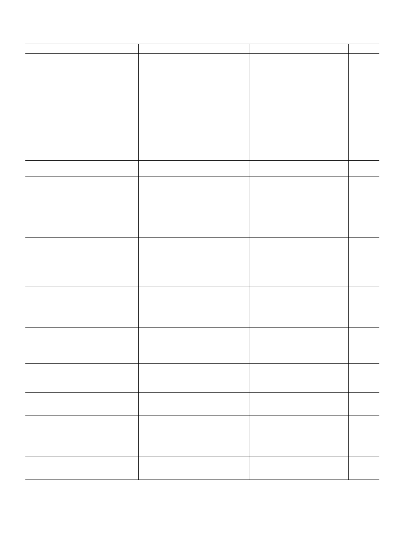
REV. 0
–2–
AD9870–SPECIFICATIONS
Parameter
Conditions
1
Min
Typ
Max
Unit
OVERALL
Analog Supply Voltage
(VDDA, VDDF, VDDI)
Digital Supply Voltage
(VDDD, VDDC, VDDL)
Interface Supply Voltage
(VDDH)
Charge Pump Supply Voltage
(VDDP, VDDQ)
Total Current
SSB Noise Figure @ Max VGA Gain
2.7
3.0
3.6
V
2.7
3.0
3.6
V
1.8
3.6
V
2.7
3.0
42
12
12
–1
–10
360
0.6
5.5
50.6
V
mA
dB
dB
dBm
dBm
dB
High IIP3 Setting
High IIP3 Setting
Low IIP3 Setting
High IIP3 Setting
Low IIP3 Setting
Input Third-Order Intercept (IIP3)
–5
Input Impedance
Gain Variation Over Temperature
PREAMP + MIXER
Maximum Input and LO Frequencies
300
MHz
LO SYNTHESIZER
LO Input Frequency
LO Input Amplitude
FREF (Reference) Frequency
FREF Input Amplitude
Minimum Charge Pump Output Current
Maximum Charge Pump Output Current
Charge Pump Output Compliance Voltage
2
Synthesizer Resolution
7.75
0.3
0.1
0.3
300
1.0
25
3
MHz
V p-p
MHz
V p-p
mA
mA
V
kHz
Programmable in 0.625 mA Steps
Programmable in 0.625 mA Steps
0.625
5.000
0.25
6.25
VDDP – 0.25
CLOCK SYNTHESIZER
CLK Input Frequency
CLK Input Amplitude
Minimum Charge Pump Output Current
Maximum Charge Pump Output Current
Charge Pump Output Compliance Voltage
2
Synthesizer Resolution
13
0.3
18
MHz
V p-p
mA
mA
V
kHz
Clock VCO Off
Programmable in 0.625 mA Steps
Programmable in 0.625 mA Steps
0.625
5.000
0.25
2.2
VDDQ – 0.25
SIGMA-DELTA ADC
Resolution
Clock Frequency (f
CLK
)
Center Frequency
Dynamic Range
Passband Gain Variation
16
Bits
MHz
MHz
dB
dB
13
18
f
CLK
/8
88
BW = 10 kHz
0.5
DECIMATOR
Decimation Factor
Passband Width
Passband Gain Variation
Alias Attenuation
Programmable in Steps of 60
60
960
50
%
dB
dB
1
85
GAIN CONTROL
Programmable Gain Step
AGC Gain Range (Continuous)
AGC Attack Time
16
25
dB
dB
μ
s
18
40
60
7000
Programmable
SPI
PC Clock Frequency
PD Hold Time
10
MHz
ns
10
SSI
CLKOUT Frequency
Output Rise/Fall Time
1
18
120
45
16
10
MHz
ns
ns
ns
ns
CMOS Output Mode, Drive Strength = 0
CMOS Output Mode, Drive Strength = 1
CMOS Output Mode, Drive Strength = 2
CMOS Output Mode, Drive Strength = 3
OPERATING TEMPERATURE RANGE
Basic Functions
Meets All Specifications
NOTES
1
Standard operating mode: high IIP3 setting, synthesizers in normal (not fast acquire) mode, f
= 18 MHz, 25 pF load on SSI output pins: VDDx = 3.0 V.
2
Voltage span in which LO (or CLK) charge pump output current is maintained within 5% of nominal value of VDDP/2 (or VDDQ/2).
Specifications subject to change without notice.
–40
–40
+95
+85
°
C
°
C
(VDDI = VDDF = VDDA = 3.3 V, VDDC = VDDL = 3.3 V, VDDD = VDDH = 3.3 V, VDDQ =
VDDP = 5.0 V, CLK = 18 MSPS, F
IF
= 73.35 MHz, F
LO
= 71.1 MHz, unless otherwise noted.)
相關(guān)PDF資料 |
PDF描述 |
|---|---|
| AD9873 | Analog Front End Converter for Set-Top Box, Cable Modem |
| AD9873-EB | Analog Front End Converter for Set-Top Box, Cable Modem |
| AD9873JS | Analog Front End Converter for Set-Top Box, Cable Modem |
| AD9874 | IF Digitizing Subsystem |
| AD9874BST | IF Digitizing Subsystem |
相關(guān)代理商/技術(shù)參數(shù) |
參數(shù)描述 |
|---|---|
| AD9873 | 制造商:AD 制造商全稱:Analog Devices 功能描述:Analog Front End Converter for Set-Top Box, Cable Modem |
| AD9873-EB | 制造商:Analog Devices 功能描述: |
| AD9873JS | 制造商:Analog Devices 功能描述: |
| AD9874 | 制造商:AD 制造商全稱:Analog Devices 功能描述:IF Digitizing Subsystem |
| AD9874ABST | 功能描述:IC IF DIGIT SUBSYSTEM 48-LQFP RoHS:否 類別:RF/IF 和 RFID >> RF 其它 IC 和模塊 系列:- 標準包裝:100 系列:* |
發(fā)布緊急采購,3分鐘左右您將得到回復。