- 您現(xiàn)在的位置:買賣IC網(wǎng) > PDF目錄373965 > AD9698TQ (ANALOG DEVICES INC) Ultrafast TTL Comparators PDF資料下載
參數(shù)資料
| 型號(hào): | AD9698TQ |
| 廠商: | ANALOG DEVICES INC |
| 元件分類: | 運(yùn)動(dòng)控制電子 |
| 英文描述: | Ultrafast TTL Comparators |
| 中文描述: | DUAL COMPARATOR, 3000 uV OFFSET-MAX, CDIP16 |
| 封裝: | CERDIP-16 |
| 文件頁(yè)數(shù): | 4/8頁(yè) |
| 文件大小: | 135K |
| 代理商: | AD9698TQ |
AD9696/AD9698
–4–
REV. B
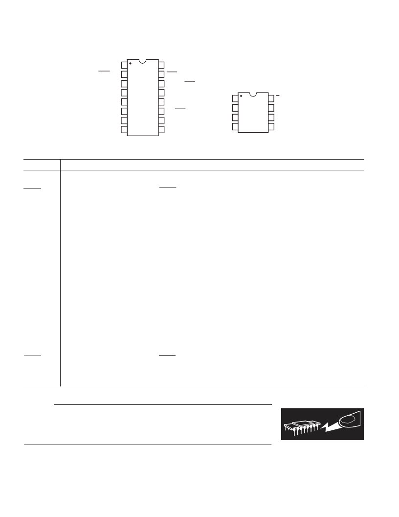
PIN CONFIGURAT IONS
AD9696KN/KR/KQ/TQ/TZ
Q1
OUT
(N/C)
Q1
OUT
(–V
S
)
GROUND (–IN
1
)
LATCH ENABLE 1 (+IN
1
)
N/C (+IN
2
)
–V
S
(–IN
2
)
–IN
1
(+V
S
)
TOP VIEW
(Not to Scale)
1
2
3
4
5
6
7
8
9
10
11
12
13
14
16
15
+IN
1
(N/C)
+IN
2
(LATCH ENABLE 2)
–IN
2
(GROUND)
N/C (Q2
OUT
)
LATCH ENABLE 2 (Q1
OUT
)
Q2
OUT
(GROUND)
Q2
OUT
(LATCH ENABLE 1)
AD9698KN/KQ/TQ
[AD9698KR/TZ PINOUTS SHOWN IN ( )]
GROUND (Q1
OUT
)
+V
S
(Q2
OUT
)
LATCH
ENABLE
1
2
3
4
TOP VIEW
(Not to Scale)
5
6
7
8
+V
S
+IN
–IN
–V
S
GROUND
Q
OUT
Q
OUT
Name
Function
Q1
OUT
One of two complementary outputs. Q1
OUT
will be at logic HIGH if voltage at +IN
1
is greater than voltage at
–IN
1
and LAT CH ENABLE 1 is at logic LOW.
One of two complementary outputs. Q1
OUT
will be at logic HIGH if voltage at –IN
1
is greater than voltage at
+IN
1
and LAT CH ENABLE 1 is at logic LOW.
Analog and digital ground return. All GROUND pins should be connected together and to a low impedance
ground plane near the comparator.
Output at Q1
OUT
will track differential changes at the inputs when LAT CH ENABLE 1 is at logic LOW.
When LAT CH ENABLE 1 is at logic HIGH, the output at Q1
OUT
will reflect the input state at the application of
the latch command, delayed by the Latch Enable Setup T ime (t
S
). Since the architecture of the input stage (see
block diagram) is faster than the logic of the latch stage, data will typically be latched if applied to the comparator(s)
within 1.7 ns after the latch. T his is the Setup T ime (t
S
); for guaranteed performance, t
S
must be 3 ns.
No internal connection to comparator.
Negative power supply connection; nominally –5.2 V.
Inverting input of differential input stage for Comparator #1.
Noninverting input of differential input stage for Comparator #1.
Noninverting input of differential input stage for Comparator #2.
Inverting input of differential input stage for Comparator #2.
Positive power supply connection; nominally +5 V.
Output at Q2
OUT
will track differential changes at the inputs when LAT CH ENABLE 2 is at logic LOW.
When LAT CH ENABLE 2 is at logic HIGH, the output at Q2
OUT
will reflect the input state at the application of
the latch command, delayed by the Latch Enable Setup T ime (t
S
). Since the architecture of the input stage (see
block diagram) is faster than the logic of the latch stage, data will typically be latched if applied to the comparator(s)
within 1.7 ns after the latch. T his is the Setup T ime (t
S
); for guaranteed performance, t
S
must be 3 ns.
One of two complementary outputs. Q2
OUT
will be at logic HIGH if voltage at –IN
2
is greater than voltage at
+IN
2
and LAT CH ENABLE 2 is at logic LOW.
One of two complementary outputs. Q2
OUT
will be at logic HIGH if voltage at +IN
2
is greater than voltage at
–IN
2
and LAT CH ENABLE 2 is at logic LOW.
Q1
OUT
GROUND
LAT CH
ENABLE 1
N/C
–V
S
–IN
1
+IN
1
+IN
2
–IN
2
+V
S
LAT CH
ENABLE 2
Q2
OUT
Q2
OUT
WARNING!
ESD SENSITIVE DEVICE
C AUT ION
ESD (electrostatic discharge) sensitive device. Electrostatic charges as high as 4000 V readily
accumulate on the human body and test equipment and can discharge without detection.
Although the AD9696/AD9698 features proprietary ESD protection circuitry, permanent dam-
age may occur on devices subjected to high energy electrostatic discharges. T herefore, proper
ESD precautions are recommended to avoid performance degradation or loss of functionality.
相關(guān)PDF資料 |
PDF描述 |
|---|---|
| AD9696 | Ultrafast TTL Comparators |
| AD9696KN | Ultrafast TTL Comparators |
| AD9696KQ | Ultrafast TTL Comparators |
| AD9696KR | Ultrafast TTL Comparators |
| AD9698 | Ultrafast TTL Comparators |
相關(guān)代理商/技術(shù)參數(shù) |
參數(shù)描述 |
|---|---|
| AD9698TQ/883B | 制造商:未知廠家 制造商全稱:未知廠家 功能描述:Analog Comparator |
| AD9698TZ/883B | 制造商:AD 制造商全稱:Analog Devices 功能描述:Ultrafast TTL Comparators |
| AD96A000Z4 | 功能描述:DIN 41612 連接器 DIN POWER CONTACT RoHS:否 制造商:HARTING 系列:har-bus 64 產(chǎn)品類型:Plugs 排數(shù):5 位置/觸點(diǎn)數(shù)量:160 安裝角:Right 類型:Shrouded Header 端接類型:Solder 外殼材料: 觸點(diǎn)材料: 觸點(diǎn)電鍍: |
| AD96A080Z4LF | 功能描述:DIN 41612 連接器 AD96A080Z4-AD RoHS:否 制造商:HARTING 系列:har-bus 64 產(chǎn)品類型:Plugs 排數(shù):5 位置/觸點(diǎn)數(shù)量:160 安裝角:Right 類型:Shrouded Header 端接類型:Solder 外殼材料: 觸點(diǎn)材料: 觸點(diǎn)電鍍: |
| AD96S | 制造商:未知廠家 制造商全稱:未知廠家 功能描述:Fast Asymmetric Thyristors |
發(fā)布緊急采購(gòu),3分鐘左右您將得到回復(fù)。