- 您現(xiàn)在的位置:買賣IC網(wǎng) > PDF目錄373959 > AD9200KST (ANALOG DEVICES INC) Complete 10-Bit, 20 MSPS, 80 mW CMOS A/D Converter PDF資料下載
參數(shù)資料
| 型號: | AD9200KST |
| 廠商: | ANALOG DEVICES INC |
| 元件分類: | ADC |
| 英文描述: | Complete 10-Bit, 20 MSPS, 80 mW CMOS A/D Converter |
| 中文描述: | 1-CH 10-BIT PROPRIETARY METHOD ADC, PARALLEL ACCESS, PQFP48 |
| 封裝: | PLASTIC, LQFP-48 |
| 文件頁數(shù): | 8/24頁 |
| 文件大?。?/td> | 338K |
| 代理商: | AD9200KST |
AD9200
–8–
REV. E
Table I. Mode Selection
Input
Connect
Input
Span
MODE
Pin
REFSENSE
Pin
Modes
REF
REFTS
REFBS
Figure
TOP/BOTTOM
AIN
1 V
AVDD
Short REFSENSE, REFTS and VREF Together
AGND
18
AIN
2 V
AVDD
AGND
Short REFTS and VREF Together
AGND
19
CENTER SPAN
AIN
1 V
AVDD/2
Short VREF and REFSENSE Together
AVDD/2
AVDD/2
20
AIN
2 V
AVDD/2
AGND
No Connect
AVDD/2
AVDD/2
Differential
AIN Is Input 1
1 V
AVDD/2
Short VREF and REFSENSE Together
AVDD/2
AVDD/2
29
REFTS and
REFBS Are
Shorted Together
for Input 2
2 V
AVDD/2
AGND
No Connect
AVDD/2
AVDD/2
External Ref
AIN
2 V max
AVDD
AVDD
No Connect
Span = REFTS
– REFBS (2 V max)
Short to
VREFTF
21, 22
AGND
Short to
VREFBF
23
AD876
AIN
2 V
Float or
AVSS
AVDD
No Connect
Short to
VREFTF
Short to
VREFBF
30
0
–9
1.0E+6
1.0E+9
10.0E+6
S
100.0E+6
–3
–6
FREQUENCY – Hz
–12
–15
–18
–21
–24
–27
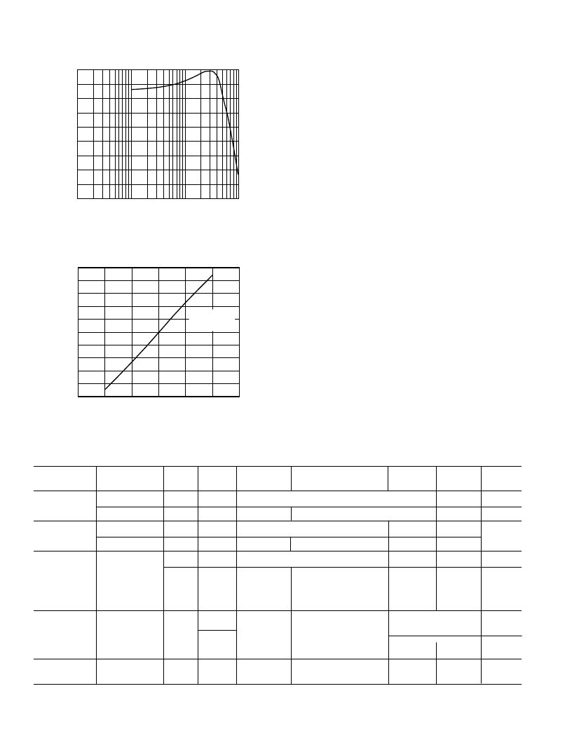
Figure 13. Full Power Bandwidth
25
20
–25
0
3.0
1.0
2.0
15
10
–5
–10
–15
INPUT VOLTAGE – V
5
0
–20
2.5
0.5
1.5
I
B
m
A
REFBS = 0.5V
REFTS = 2.5V
CLOCK = 20MHz
Figure 14. Input Bias Current vs. Input Voltage
APPLYING THE AD9200
THEORY OF OPERATION
The AD9200 implements a pipelined multistage architecture to
achieve high sample rate with low power. The AD9200 distrib-
utes the conversion over several smaller A/D subblocks, refining
the conversion with progressively higher accuracy as it passes
the results from stage to stage. As a consequence of the distrib-
uted conversion, the AD9200 requires a small fraction of the
1023 comparators used in a traditional flash type A/D. A
sample-and-hold function within each of the stages permits the
first stage to operate on a new input sample while the second,
third and fourth stages operate on the three preceding samples.
OPERATIONAL MODES
The AD9200 is designed to allow optimal performance in a
wide variety of imaging, communications and instrumentation
applications, including pin compatibility with the AD876 A/D.
To realize this flexibility, internal switches on the AD9200 are
used to reconfigure the circuit into different modes. These modes
are selected by appropriate pin strapping. There are three parts
of the circuit affected by this modality: the voltage reference, the
reference buffer, and the analog input. The nature of the appli-
cation will determine which mode is appropriate: the descrip-
tions in the following sections, as well as the Table I should
assist in picking the desired mode.
相關(guān)PDF資料 |
PDF描述 |
|---|---|
| AD9200LQFP-EVAL | Complete 10-Bit, 20 MSPS, 80 mW CMOS A/D Converter |
| AD9200JRSRL | Complete 10-Bit, 20 MSPS, 80 mW CMOS A/D Converter |
| AD9200ARSRL | Complete 10-Bit, 20 MSPS, 80 mW CMOS A/D Converter |
| AD9200 | Complete 10-Bit, 20 MSPS, 80 mW CMOS A/D Converter |
| AD9200ARS | CAP 33 UF 16V 10% |
相關(guān)代理商/技術(shù)參數(shù) |
參數(shù)描述 |
|---|---|
| AD9200KSTRL | 制造商:Rochester Electronics LLC 功能描述:- Tape and Reel 制造商:Analog Devices 功能描述: |
| AD9200KSTZ | 制造商:Analog Devices 功能描述:ADC SGL PIPELINED 20MSPS 10-BIT PARALLEL 48LQFP - Trays |
| AD9200KSTZRL | 制造商:Analog Devices 功能描述:ADC SGL PIPELINED 20MSPS 10-BIT PARALLEL 48LQFP - Tape and Reel |
| AD9200LQFP-EVAL | 制造商:AD 制造商全稱:Analog Devices 功能描述:Complete 10-Bit, 20 MSPS, 80 mW CMOS A/D Converter |
| AD9200SSOP-EVAL | 制造商:Analog Devices 功能描述:Evaluation Board For AD9200 CMOS A/D Converter 制造商:Analog Devices 功能描述:EVAL BD FOR AD9200 CMOS A/D CNVRTR - Bulk |
發(fā)布緊急采購,3分鐘左右您將得到回復(fù)。