- 您現(xiàn)在的位置:買賣IC網(wǎng) > PDF目錄375239 > AD7829 (Analog Devices, Inc.) 8-Channel Sampling ADCs(2MSPS,8通道采樣8位A/D轉(zhuǎn)換器) PDF資料下載
參數(shù)資料
| 型號: | AD7829 |
| 廠商: | Analog Devices, Inc. |
| 英文描述: | 8-Channel Sampling ADCs(2MSPS,8通道采樣8位A/D轉(zhuǎn)換器) |
| 中文描述: | 8通道采樣ADC(2MSPS,8通道采樣8位的A / D轉(zhuǎn)換器) |
| 文件頁數(shù): | 9/20頁 |
| 文件大小: | 238K |
| 代理商: | AD7829 |
AD7822/AD7825/AD7829
–9–
REV. 0
AD7822/25/29
V
REF
V
MID
V
IN
2.5V
R3
R4
R2
R1
V
V
0V
V
IN
0V
2.5V
Figure 9. Accommodating Bipolar Signals Using
External V
MID
AD7822/25/29
V
REF
V
MID
V
IN
EXTERNAL
2.5V
R3
R4
R2
R1
V
V
0V
V
IN
0V
V
MID
Figure 10. Accommodating Bipolar Signals Using
Internal V
MID
NOT E: Although there is a V
REF
pin from which a voltage
reference of 2.5 V may be sourced, or to which an external
reference may be applied, this does not provide an option of
varying the value of the voltage reference. As stated in the
specifications for the AD7822, AD7825 and AD7829, the input
voltage range at this pin is 2.5 V
±
2%.
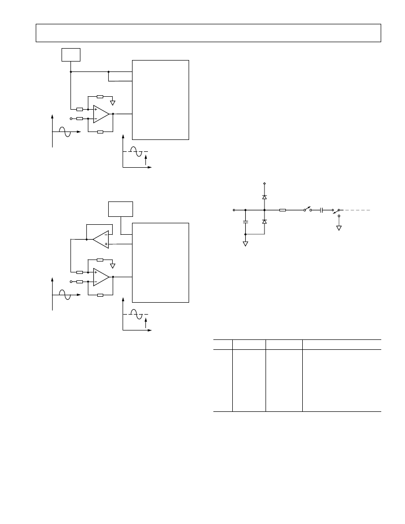
Analog Input Structure
Figure 11 shows an equivalent circuit of the analog input struc-
ture of the AD7822, AD7825 and the AD7829. T he two diodes,
D1 and D2, provide ESD protection for the analog inputs.
Care must be taken to ensure that the analog input signal never
exceeds the supply rails by more than 200 mV. T his will cause
these diodes to become forward biased and start conducting
current into the substrate. 20 mA is the maximum current these
diodes can conduct without causing irreversible damage to the
part. However, it is worth noting that a small amount of current
(1 mA) being conducted into the substrate due to an over volt-
age on an unselected channel, can cause inaccurate conversions
on a selected channel. T he capacitor C2 in Figure 11 is typically
about 4 pF and can be primarily attributed to pin capacitance.
T he resistor, R1, is a lumped component made up of the on
resistance of several components, including that of the multi-
plexer and the track and hold. T his resistor is typically about
310
. T he capacitor C1 is the track-and-hold capacitor and has
a capacitance of 0.5 pF. Switch 1 is the track-and-hold switch,
while Switch 2 is that of the sampling capacitor as shown in
Figures 2 and 3.
When in track phase, Switch 1 is closed and Switch 2 is in
Position A; when in hold mode, Switch 1 opens while Switch
2 remains in Position A. T he track-and-hold remains in hold
mode for 120 ns—see Circuit Description, after which it returns
to track mode and the ADC enters its conversion phase. At this
point Switch 1 opens and Switch 2 moves to Position B. At the
end of the conversion Switch 2 moves back to Position A.
V
IN
C2
4pF
D1
D2
R1
310
V
SW1
C1
0.5pFA
B
SW2
V
DD
Figure 11. Equivalent Analog Input Circuit
Analog Input Selection
On power-up, the default V
IN
selection is V
IN1
. When returning
to normal operation from power-down, the V
IN
selected will be
the same one that was selected prior to power-down being initi-
ated. T able II below shows the multiplexer address correspond-
ing to each analog input from V
IN1
to V
IN4(8)
for the AD7825 or
AD7829.
T able II.
A2
A1
A0
Analog Input Selected
0
0
0
0
1
1
1
1
0
0
1
1
0
0
1
1
0
1
0
1
0
1
0
1
V
IN1
V
IN2
V
IN3
V
IN4
V
IN5
V
IN6
V
IN7
V
IN8
Channel selection on the AD7825 and AD7829 is made without
the necessity of a write operation. T he address of the
next
chan-
nel to be converted is latched at the start of the
current
read
operation, as shown in Figure 12. T his allows for improved
throughput rates in “channel hopping” applications.
相關(guān)PDF資料 |
PDF描述 |
|---|---|
| AD7823 | 8-Bit ADC in 8-Lead microSOIC/DIP(8位A/D轉(zhuǎn)換器) |
| AD7824 | High Speed 4-Channel 8-Bit ADC(四通道LC2MOS高速8位A/D轉(zhuǎn)換器) |
| AD7834AN | 2.35V-5.25V, 12 bit, 1MSPS, Serial ADC 6-SOT-23 -40 to 125 |
| AD7834AR | 2.35V-5.25V, 12 bit, 1MSPS, Serial ADC 6-SOT-23 -40 to 125 |
| AD7834BN | 2.35V-5.25V, 12 bit, 1MSPS, Serial ADC 6-SC70 -40 to 125 |
相關(guān)代理商/技術(shù)參數(shù) |
參數(shù)描述 |
|---|---|
| AD7829-1 | 制造商:AD 制造商全稱:Analog Devices 功能描述:3 V/5 V, 2 MSPS, 8-Bit, 8-Channel ADC |
| AD7829BN | 制造商:Analog Devices 功能描述:ADC Single Semiflash 2Msps 8-bit Parallel 28-Pin PDIP W 制造商:Rochester Electronics LLC 功能描述:8-CHNL 2MSPS PARALLEL 8-BIT ADC I.C. - Bulk 制造商:Analog Devices 功能描述:IC 8BIT ADC 7829 DIP28 |
| AD7829BNZ | 制造商:Analog Devices 功能描述:ADC Single Semiflash 2Msps 8-bit Parallel 28-Pin PDIP W 制造商:Analog Devices 功能描述:IC 8BIT ADC 7829 DIP28 |
| AD7829BNZ1 | 制造商:AD 制造商全稱:Analog Devices 功能描述:3 V/5 V, 2 MSPS, 8-Bit, 1-/4-/8-Channel Sampling ADCs |
| AD7829BR | 制造商:Rochester Electronics LLC 功能描述:8-CHNL 2MSPS PARALLEL 8-BIT ADC I.C. - Bulk 制造商:Analog Devices 功能描述:IC 8-BIT ADC |
發(fā)布緊急采購,3分鐘左右您將得到回復(fù)。