- 您現(xiàn)在的位置:買賣IC網(wǎng) > PDF目錄375239 > AD7816 (Analog Devices, Inc.) 10-Bit ADCs with On-Chip Temperature Sensor(10位A/D轉換器) PDF資料下載
參數(shù)資料
| 型號: | AD7816 |
| 廠商: | Analog Devices, Inc. |
| 元件分類: | 溫度/濕度傳感器 |
| 英文描述: | 10-Bit ADCs with On-Chip Temperature Sensor(10位A/D轉換器) |
| 中文描述: | 10位ADC的片上溫度傳感器(10位的A / D轉換器) |
| 文件頁數(shù): | 15/16頁 |
| 文件大?。?/td> | 230K |
| 代理商: | AD7816 |
AD7816/AD7817/AD7818
–15–
REV. 0
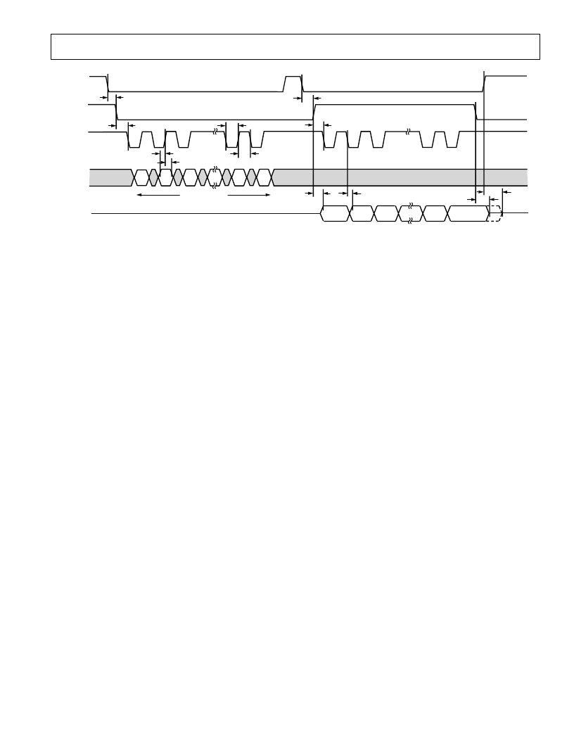
Read Operation
Figure 20 shows the timing diagram for a serial read from the
AD7817.
CS
is brought low to enable the serial interface and
RD/
WR
is set logic high to indicate that the data transfer is a
serial read from the AD7817. The rising edge of RD/
WR
clocks
out the first data bit (DB9), subsequent bits are clocked out on
the falling edge of SCLK and are valid on the rising edge. Ten
bits of data are transferred during a read operation. However,
the user has the choice of clocking only eight bits if the full ten
bits of the conversion result are not required. The serial data can
be accessed in a number of bytes if ten bits of data are being
read. However, RD/
WR
must remain high for the duration of
the data transfer operation. Before starting a new data read
operation the RD/
WR
signal must brought low and high again.
At the end of the read operation, the D
OUT
line enters a high
impedance state on the rising edge of the
CS
or the falling edge
of RD/
WR
, whichever occurs first.
Write Operation
Figure 20 also shows a control byte write operation to the
AD7817. The RD/
WR
input goes low to indicate to the part
that a serial write is about to occur. The AD7817 control byte
is loaded on the rising edge of the first eight clock cycles of the
serial clock with data on all subsequent clock cycles being ig-
nored. To carry out a second successive write operation, the
RD/
WR
signal must be brought high and low again.
Simplifying the Serial Interface
To minimize the number of interconnect lines to the AD7817,
the user can connect the
CS
line to DGND. This is possible if
the AD7817 is not sharing the serial bus with another device. It
is also possible to tie the D
IN
and D
OUT
lines together. This
arrangement is compatible with the 8051 microcontroller. The
68HC11, 68HC05 and PIC16Cxx can be configured to operate
with a single serial data line. In this way the number of lines
required to operate the serial interface can be reduced to three,
i.e., RD/
WR
, SCLK and D
IN/OUT
—see Figure 6.
AD7816 AND AD7818 SERIAL INTERFACE MODE
The serial interface on the AD7816 and AD7818 is a three-wire
interface with read and write capabilities. Data is read from the
output register and the control byte is written to the AD7816
DB9
DB8
DB7
DB0
DB1
DB8
DB7
DB6
DB1
DB0
SCLK
D
IN
1
3
2
1
2
3
9
10
RD/
WR
CS
t
4
t
7
t
10
t
14a
t
14b
t
13
t
12
t
11
t
8
t
9
t
5
t
6
8
7
CONTROL BYTE
D
OUT
Figure 20. AD7817 Serial Interface Timing Diagram
and AD7818 via the D
IN/OUT
line. The part operates in a slave
mode and requires an externally applied serial clock to the
SCLK input to access data from the data register or write the
control byte. The RD/
WR
line is used to determine whether
data is being written to or read from the AD7816 and AD7818.
When data is being written to the devices the RD/
WR
line is set
logic low and when data is being read from the part the line is
set logic high—see Figure 21. The serial interface on the
AD7816 and AD7818 are designed to allow the part to be inter-
faced to systems that provide a serial clock that is synchronized
to the serial data, such as the 80C51, 87C51, 68HC11, 68HC05
and PIC16Cxx microcontrollers.
Read Operation
Figure 21 shows the timing diagram for a serial read from the
AD7816 and AD7818. The RD/
WR
is set logic high to indicate
that the data transfer is a serial read from the devices. When
RD/
WR
is logic high the D
IN/OUT
pin becomes a logic output
and the first data bit (DB9) appears on the pin. Subsequent bits
are clocked out on the falling edge of SCLK, starting with the
second SCLK falling edge after RD/
WR
goes high and are valid
on the rising edge of SCLK. Ten bits of data are transferred
during a read operation. However the user has the choice of
clocking only eight bits if the full ten bits of the conversion
result are not required. The serial data can be accessed in a
number of bytes if ten bits of data are being read; however,
RD/
WR
must remain high for the duration of the data transfer
operation. To carry out a successive read operation the RD/
WR
pin must be brought logic low and high again. At the end of the
read operation, the D
IN/OUT
pin becomes a logic input on the
falling edge of RD/
WR
.
Write Operation
A control byte write operation to the AD7816 and AD7818 is
also shown in Figure 21. The RD/
WR
input goes low to indicate
to the part that a serial write is about to occur. The AD7816
and AD7818 control bytes are loaded on the rising edge of the
first eight clock cycles of the serial clock with data on all subse-
quent clock cycles being ignored. To carry out a successive write
to the AD7816 or AD7818 the RD/
WR
pin must be brought
logic high and low again.
相關PDF資料 |
PDF描述 |
|---|---|
| AD7817 | 10-Bit ADCs with On-Chip Temperature Sensor(四通道,10位A/D轉換器) |
| AD7818 | 10-Bit ADCs with On-Chip Temperature Sensor(單通道,10位A/D轉換器) |
| AD7819 | 8-Bit Sampling ADC(200kSPS,8位采樣A/D轉換器) |
| AD7820 | LC2MOS HIGH-SPEED uP-COMPATIBLE 8-BIT ADC WITH TRACK/HOLD FUNCTION |
| AD7820BQ | LC2MOS HIGH-SPEED uP-COMPATIBLE 8-BIT ADC WITH TRACK/HOLD FUNCTION |
相關代理商/技術參數(shù) |
參數(shù)描述 |
|---|---|
| AD7816-7818 | 制造商:AD 制造商全稱:Analog Devices 功能描述:Single- and 4-Channel, 9 us, 10-Bit ADCs with On-Chip Temperature Sensor |
| AD7816ACHIPS | 制造商:AD 制造商全稱:Analog Devices 功能描述:Single- and 4-Channel, 9 us, 10-Bit ADCs with On-Chip Temperature Sensor |
| AD7816AR | 制造商:Analog Devices 功能描述:Analog Temperature Sensors 8-Pin SOIC N 制造商:Rochester Electronics LLC 功能描述:TEMP SENSOR I.C. - Bulk 制造商:Analog Devices 功能描述:ADC TEMP SENSOR SMD 7816 SOIC8 |
| AD7816ARM | 制造商:Analog Devices 功能描述:Analog Temperature Sensors 8-Pin MSOP 制造商:Rochester Electronics LLC 功能描述:TEMPERATURE SENSOR: 10-BIT ADC, TEMPERATURE MONITORING ONLY - Bulk |
| AD7816ARM-REEL | 制造商:Analog Devices 功能描述:Analog Temperature Sensors 8-Pin MSOP T/R 制造商:Rochester Electronics LLC 功能描述:TEMPERATURE SENSOR: 10-BIT ADC, TEMPERATURE MONITORING ONLY - Tape and Reel |
發(fā)布緊急采購,3分鐘左右您將得到回復。