- 您現(xiàn)在的位置:買賣IC網(wǎng) > PDF目錄375235 > AD7010 (Analog Devices, Inc.) CMOS JDC DQPSK Baseband Transmit Port(CMOS 基帶傳輸口) PDF資料下載
參數(shù)資料
| 型號(hào): | AD7010 |
| 廠商: | Analog Devices, Inc. |
| 英文描述: | CMOS JDC DQPSK Baseband Transmit Port(CMOS 基帶傳輸口) |
| 中文描述: | 聯(lián)合紀(jì)律委員會(huì)DQPSK的CMOS基帶傳輸端口(的CMOS基帶傳輸口) |
| 文件頁數(shù): | 5/8頁 |
| 文件大小: | 257K |
| 代理商: | AD7010 |
AD7010
REV. B
–5–
PIN FUNCT ION DE SCRIPT ION
SSOP Pin
Number
Mnemonic
Function
POWE R SUPPLY
19
5
14, 18, 23
6
ANALOG SIGNAL AND RE FE RE NCE
13
BYPASS
V
AA
V
DD
AGND
DGND
Positive power supply for analog section.
Positive power supply for digital section, both supplies should be externally tied together.
Analog ground for transmit section.
Digital ground for transmit section, both grounds should be externally tied together.
Reference decoupling output. A decoupling capacitor should be connected between this pin a
and AGND.
Differential analog outputs for the I channel, representing true and complementary outputs
of the I waveform.
Differential analog outputs for the Q channel, representing true and complementary outputs
of the Q waveform.
T RANSMIT INT E RFACE AND CONT ROL
7
MCLK
Master clock, digital input. T his pin should be driven by a 2.688 MHz CMOS compatible
clock source in digital mode.
3
T xCLK
T his is a digital output, transmit clock. T his may be used to clock in transmit data at 42 kHz.
4
T xDAT A
T his is a digital input. T his pin is used to clock in transmit data on the falling edge of T xCLK
at a rate of 42 kHz.
2
BIN
T his is a digital input. T his input is used to initiate the ramping up (BIN high) or down (BIN
low) of the I and Q waveforms.
24
BOUT
Burst out, digital output. T his is the BIN input delayed by the pipeline delay, both digital and
analog, of the AD7010. T his can be used to turn on and off the RF amplifiers in synchroniza-
tion with the I and Q waveforms.
1
POWER
T ransmit sleep mode, digital input. When this goes low, the AD7010 goes into sleep mode,
drawing minimal current. When this pin goes high, the AD7010 is brought out of sleep mode
and initiates a self-calibration routine to eliminate the offset between IT x &
ITx
and the offset
between QT x &
QTx
.
12
READY
T ransmit ready, digital output. T his output goes high once the self-calibration routine is complete.
9, 11
MODE1,
Mode control, digital inputs. T hese are used to enter the AD7010 into three different
MODE2
operating modes, see T able I.
8, 10, 15, 22
NC
No Connects. T hese pins are no connects and should not be used as routes for other circuit signals.
16, 17
IT x,
ITx
21, 20
QT x,
QTx
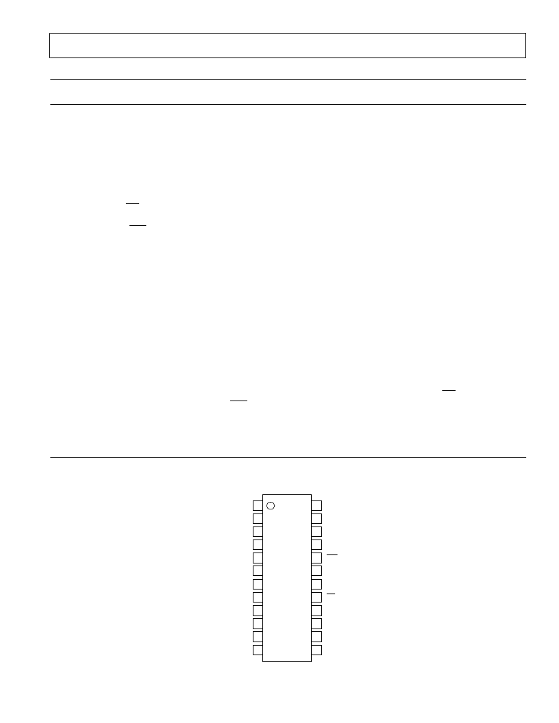
SSOP PIN CONFIGURAT ION
POWER
BIN
TxCLK
TxDATA
V
DD
DGND
MCLK
MODE1
NC
BOUT
AGND
QTx
QTx
V
AA
AGND
ITx
ITx
AGND
BYPASS
1
2
3
7
24
23
22
18
8
9
10
17
16
15
11
12
14
13
4
5
21
20
6
19
TOP VIEW
(Not to Scale)
AD7010
NC
MODE2
READY
NC
NC
相關(guān)PDF資料 |
PDF描述 |
|---|---|
| AD7011 | CMOS, ADC p/4 DQPSK Baseband Transmit Port |
| AD7011ARS | MB 4C 4#12 PIN RECP |
| AD7013ARS | CMOS TIA IS-54 Baseband Receive Port |
| AD7013 | CMOS TIA IS-54 Baseband Receive Port(CMOS 基帶接收口) |
| AD7015 | Complete 3 V GSM/DCS1800 Codec(GSM/DCS1800 編碼譯碼器) |
相關(guān)代理商/技術(shù)參數(shù) |
參數(shù)描述 |
|---|---|
| AD7010ARS | 制造商:AD 制造商全稱:Analog Devices 功能描述:CMOS JDC p/4 DQPSK Baseband Transmit Port |
| AD7011 | 制造商:AD 制造商全稱:Analog Devices 功能描述:CMOS, ADC p/4 DQPSK Baseband Transmit Port |
| AD7011ARS | 制造商:Analog Devices 功能描述:Quadrature Mod 24-Pin SSOP |
| AD7011ARS-REEL | 制造商:Analog Devices 功能描述:Quadrature Mod 24-Pin SSOP T/R 制造商:Rochester Electronics LLC 功能描述:- Tape and Reel |
| AD7013 | 制造商:AD 制造商全稱:Analog Devices 功能描述:CMOS TIA IS-54 Baseband Receive Port |
發(fā)布緊急采購,3分鐘左右您將得到回復(fù)。