- 您現(xiàn)在的位置:買賣IC網(wǎng) > PDF目錄375233 > AD5539 (Analog Devices, Inc.) Ultrahigh Frequency Operational Amplifier(超高頻率運算放大器) PDF資料下載
參數(shù)資料
| 型號: | AD5539 |
| 廠商: | Analog Devices, Inc. |
| 英文描述: | Ultrahigh Frequency Operational Amplifier(超高頻率運算放大器) |
| 中文描述: | 超高頻率運算放大器(超高頻率運算放大器) |
| 文件頁數(shù): | 6/16頁 |
| 文件大小: | 499K |
| 代理商: | AD5539 |
AD5539
REV. B
–6–
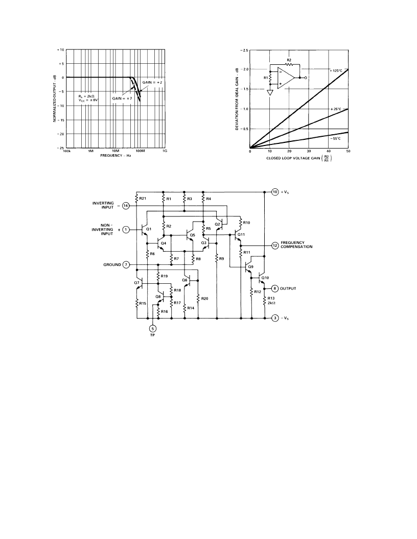
FUNCT IONAL DE SCRIPT ION
T he AD5539 is a two-stage, very high frequency amplifier.
Darlington input transistors Q1, Q4–Q2, Q3 form the first
stage—a differential gain amplifier with a voltage gain of ap-
proximately 50. T he second stage, Q5, is a single-ended ampli-
fier whose input is derived from one phase of the differential
amplifier output; the other phase of the differential output is
then summed with the output of Q5. T he all NPN design of the
AD5539 is configured such that the emitter of Q5 is returned,
via a small resistor to ground; this eliminates the need for sepa-
rate level shifting circuitry.
T he output stage, consisting of transistors Q9 and Q10, is a
Darlington voltage follower with a resistive pull-down. T he bias
section, consisting of transistors Q6, Q7 and Q8, provides a
stable emitter current for the input section, compensating for
temperature and power supply variations.
SOME GE NE RAL PRINCIPLE S OF HIGH FRE QUE NCY
CIRCUIT DE SIGN
In designing practical circuits with the AD5539, the user must
remember that whenever very high frequencies are involved,
some special precautions are in order. All real-world applica-
tions circuits must be built using proper RF techniques: the use
of short interconnect leads, adequate shielding, groundplanes,
and very low profile IC sockets. In addition, very careful bypass-
ing of power supply leads is a must.
Low-impedance transmission line is frequently used to carry sig-
nals at RF frequencies: 50
line for telecommunications pur-
poses and 75
for video applications. T he AD5539 offers a
relatively low output impedance; therefore, some consideration
must be given to impedance matching. A common matching
technique involves simply placing a resistor in series with the
amplifier output that is equal to the characteristic impedance of
the transmission line. T his provides a good match (although at a
loss of 6 dB), adequate for many applications.
All of the circuits here were built and tested in a 50
system.
Care should be taken in adapting these circuits for each particu-
lar use. Any system which has been properly matched and ter-
minated in its characteristic impedance should have the same
small signal frequency response as those shown in this
data sheet.
Figure 11. Deviation from Ideal Gain
vs. Closed-Loop Voltage Gain
Figure 10. Full Power Response
Figure 12. AD5539 Circuit
相關(guān)PDF資料 |
PDF描述 |
|---|---|
| AD5547 | Dual Current Output, Parallel Input, 16-/14-Bit Multiplying DACs with 4-Quadrant Resistors |
| AD5547BRU | Dual Current Output, Parallel Input, 16-/14-Bit Multiplying DACs with 4-Quadrant Resistors |
| AD5547BRU-REEL7 | Dual Current Output, Parallel Input, 16-/14-Bit Multiplying DACs with 4-Quadrant Resistors |
| AD5557 | Dual Current Output, Parallel Input, 16-/14-Bit Multiplying DACs with 4-Quadrant Resistors |
| AD5557CRU | Dual Current Output, Parallel Input, 16-/14-Bit Multiplying DACs with 4-Quadrant Resistors |
相關(guān)代理商/技術(shù)參數(shù) |
參數(shù)描述 |
|---|---|
| AD5539J | 制造商:AD 制造商全稱:Analog Devices 功能描述:Ultrahigh Frequency Operational Amplifier |
| AD5539JN | 制造商:未知廠家 制造商全稱:未知廠家 功能描述:Voltage-Feedback Operational Amplifier |
| AD5539JQ | 制造商:Rochester Electronics LLC 功能描述:- Bulk |
| AD5539S | 制造商:AD 制造商全稱:Analog Devices 功能描述:Ultrahigh Frequency Operational Amplifier |
| AD5539SQ | 制造商:AD 制造商全稱:Analog Devices 功能描述:Ultrahigh Frequency Operational Amplifier |
發(fā)布緊急采購,3分鐘左右您將得到回復(fù)。