- 您現(xiàn)在的位置:買賣IC網(wǎng) > PDF目錄9301 > AD5245BRJZ5-R2 (Analog Devices Inc)IC DGTL POT 256POS SOT-23-8 T/R PDF資料下載
參數(shù)資料
| 型號(hào): | AD5245BRJZ5-R2 |
| 廠商: | Analog Devices Inc |
| 文件頁(yè)數(shù): | 6/20頁(yè) |
| 文件大?。?/td> | 0K |
| 描述: | IC DGTL POT 256POS SOT-23-8 T/R |
| 標(biāo)準(zhǔn)包裝: | 1 |
| 接片: | 256 |
| 電阻(歐姆): | 5k |
| 電路數(shù): | 1 |
| 溫度系數(shù): | 標(biāo)準(zhǔn)值 45 ppm/°C |
| 存儲(chǔ)器類型: | 易失 |
| 接口: | I²C(設(shè)備位址) |
| 電源電壓: | 2.7 V ~ 5.5 V |
| 工作溫度: | -40°C ~ 125°C |
| 安裝類型: | 表面貼裝 |
| 封裝/外殼: | SOT-23-8 |
| 供應(yīng)商設(shè)備封裝: | SOT-23-8 |
| 包裝: | 剪切帶 (CT) |
| 其它名稱: | AD5245BRJZ5-R2CT |
第1頁(yè)第2頁(yè)第3頁(yè)第4頁(yè)第5頁(yè)當(dāng)前第6頁(yè)第7頁(yè)第8頁(yè)第9頁(yè)第10頁(yè)第11頁(yè)第12頁(yè)第13頁(yè)第14頁(yè)第15頁(yè)第16頁(yè)第17頁(yè)第18頁(yè)第19頁(yè)第20頁(yè)
AD5245
Rev. B | Page 14 of 20
PROGRAMMING THE POTENTIOMETER DIVIDER
Voltage Output Operation
The digital potentiometer easily generates a voltage divider at
wiper-to-B and wiper-to-A proportional to the input voltage at
A to B. Unlike the polarity of VDD to GND, which must be
positive, voltage across A to B, W to A, and W to B can be at
either polarity.
A
VI
W
B
VO
03
43
6-
0
3
6
Figure 37. Potentiometer Mode Configuration
If ignoring the effect of the wiper resistance for approximation,
then connecting the A terminal to 5 V and the B terminal to
ground produces an output voltage at the wiper-to-B starting at
0 V up to 1 LSB less than 5 V. Each LSB of voltage is equal to the
voltage applied across Terminal A and B divided by the 256
positions of the potentiometer divider. The general equation
defining the output voltage at VW with respect to ground for any
valid input voltage applied to Terminals A and B is
B
A
W
V
D
V
D
V
256
)
(
+
=
(3)
A more accurate calculation, which includes the effect of wiper
resistance, VW, is
B
AB
WA
A
AB
WB
W
V
R
D
R
V
R
D
R
D
V
)
(
)
(
)
(
+
=
(4)
Operation of the digital potentiometer in the divider mode
results in a more accurate operation over temperature. Unlike
the rheostat mode, the output voltage is dependent mainly on
the ratio of the internal resistors, RWA and RWB, not the absolute
values. Therefore, the temperature drift reduces to 15 ppm/°C.
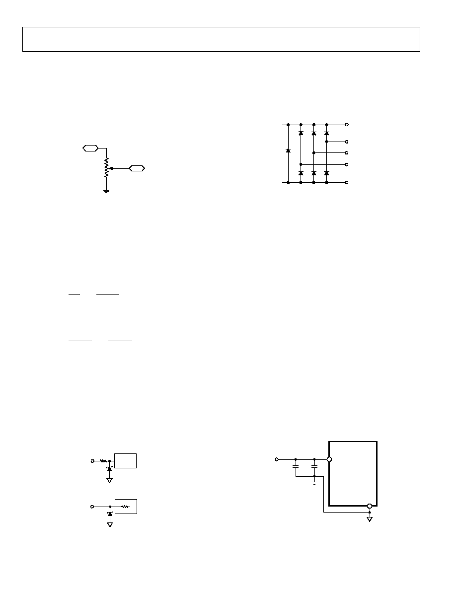
ESD PROTECTION
All digital inputs are protected with a series of input resistors and
parallel Zener ESD structures, shown in Figure 38 and Figure 39.
This applies to the digital input pins SDA, SCL, and AD0.
LOGIC
340
GND
0
34
36
-0
3
7
Figure 38. ESD Protection of Digital Pins
A, B, W
GND
0
343
6-
03
8
Figure 39. ESD Protection of Resistor Terminals
TERMINAL VOLTAGE OPERATING RANGE
The AD5245 VDD and GND power supply defines the boundary
conditions for proper 3-terminal digital potentiometer
operation. Supply signals present on Terminals A, B, and W that
exceed VDD or GND are clamped by the internal forward-biased
diodes (see Figure 40).
GND
A
W
B
VDD
03
43
6
-03
9
Figure 40. Maximum Terminal Voltages Set by VDD and GND
POWER-UP SEQUENCE
Because the ESD protection diodes limit the voltage compliance
at Terminals A, B, and W (see Figure 40), it is important to
power VDD and GND before applying any voltage to Terminals
A, B, and W; otherwise, the diode is forward biased such that
VDD is powered unintentionally and can affect the rest of the
user’s circuit. The ideal power-up sequence is in the following
order: GND, VDD, digital inputs, and then VA, VB, and VW. The
relative order of powering VA, VB, VW, and the digital inputs is
not important as long as they are powered after VDD and GND.
LAYOUT AND POWER SUPPLY BYPASSING
It is good practice to employ compact, minimum lead length
layout design. The leads to the inputs should be as direct as
possible with a minimum conductor length. Ground paths
should have low resistance and low inductance.
Similarly, it is also good practice to bypass the power supplies
with quality capacitors for optimum stability. Supply leads to
the device should be bypassed with disk or chip ceramic
capacitors of 0.01 F to 0.1 F. Low ESR 1 F to 10 F tantalum
or electrolytic capacitors should also be applied at the supplies
to minimize any transient disturbance and low frequency ripple
(see Figure 41). Note that the digital ground should also be
joined remotely to the analog ground at one point to minimize
the ground bounce.
VDD
GND
VDD
C3
10F
C1
0.1F
AD5245
+
03
43
6
-04
0
Figure 41. Power Supply Bypassing
相關(guān)PDF資料 |
PDF描述 |
|---|---|
| VE-B6L-MY-F2 | CONVERTER MOD DC/DC 28V 50W |
| VE-B6L-MY-F1 | CONVERTER MOD DC/DC 28V 50W |
| VE-B6K-MY-F4 | CONVERTER MOD DC/DC 40V 50W |
| VE-B6K-MY-F3 | CONVERTER MOD DC/DC 40V 50W |
| AD5245BRJZ50-R2 | IC DGTL POT 256POS SOT-23-8 T/R |
相關(guān)代理商/技術(shù)參數(shù) |
參數(shù)描述 |
|---|---|
| AD5245BRJZ5-R2 | 制造商:Analog Devices 功能描述:IC DIGITAL POT 5KOHM 256 SGL SOT23-8 |
| AD5245BRJZ5-R21 | 制造商:AD 制造商全稱:Analog Devices 功能描述:256-Position I2C-Compatible Digital Potentiometer |
| AD5245BRJZ5-RL7 | 功能描述:IC POT DGTL 5K 256POS SOT23-8 RoHS:是 類別:集成電路 (IC) >> 數(shù)據(jù)采集 - 數(shù)字電位器 系列:- 產(chǎn)品培訓(xùn)模塊:Lead (SnPb) Finish for COTS Obsolescence Mitigation Program 標(biāo)準(zhǔn)包裝:1 系列:- 接片:256 電阻(歐姆):100k 電路數(shù):1 溫度系數(shù):標(biāo)準(zhǔn)值 35 ppm/°C 存儲(chǔ)器類型:非易失 接口:3 線串口 電源電壓:2.7 V ~ 5.25 V 工作溫度:-40°C ~ 85°C 安裝類型:表面貼裝 封裝/外殼:8-WDFN 裸露焊盤 供應(yīng)商設(shè)備封裝:8-TDFN-EP(3x3) 包裝:剪切帶 (CT) 產(chǎn)品目錄頁(yè)面:1399 (CN2011-ZH PDF) 其它名稱:MAX5423ETA+TCT |
| AD5245BRJZ5-RL71 | 制造商:AD 制造商全稱:Analog Devices 功能描述:256-Position I2C-Compatible Digital Potentiometer |
| AD5245EVAL | 制造商:Analog Devices 功能描述:Development Tools, 256-Position I2C Compatible Digital Potentiometer 制造商:Analog Devices 功能描述:AD5245 EVAL BOARD - Bulk |
發(fā)布緊急采購(gòu),3分鐘左右您將得到回復(fù)。