- 您現(xiàn)在的位置:買賣IC網(wǎng) > PDF目錄375142 > A49LF040A (AMIC Technology Corporation) 4 Mbit CMOS 3.3Volt-only Low Pin Count Flash Memory PDF資料下載
參數(shù)資料
| 型號(hào): | A49LF040A |
| 廠商: | AMIC Technology Corporation |
| 英文描述: | 4 Mbit CMOS 3.3Volt-only Low Pin Count Flash Memory |
| 中文描述: | 4兆位的CMOS 3.3Volt只低引腳數(shù)快閃記憶體 |
| 文件頁(yè)數(shù): | 13/32頁(yè) |
| 文件大?。?/td> | 622K |
| 代理商: | A49LF040A |
第1頁(yè)第2頁(yè)第3頁(yè)第4頁(yè)第5頁(yè)第6頁(yè)第7頁(yè)第8頁(yè)第9頁(yè)第10頁(yè)第11頁(yè)第12頁(yè)當(dāng)前第13頁(yè)第14頁(yè)第15頁(yè)第16頁(yè)第17頁(yè)第18頁(yè)第19頁(yè)第20頁(yè)第21頁(yè)第22頁(yè)第23頁(yè)第24頁(yè)第25頁(yè)第26頁(yè)第27頁(yè)第28頁(yè)第29頁(yè)第30頁(yè)第31頁(yè)第32頁(yè)
A49LF040A
PRELIMINARY (March, 2006, Version 0.1)
12
AMIC Technology, Corp.
ADDRESS/ADDRESS MULTIPLEXED (A/A MUX)
MODE
Device Operation
Commands are used to initiate the memory operation
functions of the device. The data portion of the software
command sequence is latched on the rising edge of
WE
.
During the software command sequence the row address is
latched on the falling edge of
R/
latched on the rising edge of
Table 11 for operation modes and the command sequence.
C
R/
and the column address is
C
. Refer to Table 10 and
Read
The Read operation of the A49LF040A device is controlled
by OE . OE is the output control and is used to gate data
from the output pins. Refer to the Read cycle timing diagram,
Figure 10 for further details.
Reset
A V
IL
on RST pin initiates a device reset.
Byte-Program Operation
The A49LF040A device is programmed on a byte-by-byte
basis. Before programming, one must ensure that the block,
in which the byte which is being programmed exists, is fully
erased. The Byte-Program operation is initiated by executing
a four-byte command load sequence for Software Data
Protection with address and data in the last byte sequence.
During the Byte-Program operation, the row address (A10-A0)
is latched on the falling edge of
(A18-A11) is latched on the rising edge of
is latched in the rising edge of
WE
. See Figure 11 for
Program operation timing diagram, Figure 14 for timing
waveforms, and Figure 19 for its flowchart. During the
Program operation, the only valid reads are
Data
Polling and
Toggle Bit. During the internal Program operation, the host is
free to perform additional tasks. Any commands written
during the internal Program operation will be ignored.
C
R/
and the column Address
C
R/
. The data bus
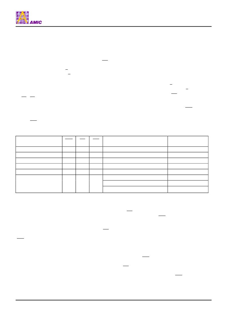
Table 10: A/A Mux Mode Operation Selection
Block-Erase Operation
The Block-Erase Operation allows the system to erase the
device in 64 KByte uniform block size for the A49LF040A.
The Block-Erase operation is initiated by executing a six-byte
command load sequence for Software Data Protection with
Block-Erase command (30H or 50H) and block address. The
internal Block-Erase operation begins after the sixth
WE
pulse. The End-of-Erase can be determined using either
Data
Polling or Toggle Bit methods. See Figure 15 for timing
waveforms. Any commands written during the Block- Erase
operation will be ignored.
Chip-Erase
The A49LF040A device provides a Chip-Erase operation
only in A/A Mux mode, which allows the user to erase the
entire memory array to the ‘1’s state. This is useful when the
entire device must be quickly erased. The Chip-Erase
operation is initiated by executing a six-byte Software Data
Protection command sequence with Chip-Erase command
(10H) with address 5555H in the last byte sequence. The
internal Erase operation begins with the rising edge of the
sixth
WE
. During the internal Erase operation, the only
valid read is Toggle Bit or
Data
Polling. See Table 11 for the
command sequence, Figure 16 for timing diagram, and
Figure 21 for the flowchart. Any commands written during the
Chip-Erase operation will be ignored.
Write Operation Status Detection
The A49LF040A device provides two software means to
detect the completion of a Write cycle, in order to optimize
the system Write cycle time. The software detection includes
two status bits:
Data
Polling (I/O
7
) and Toggle Bit (I/O
6
). The
End-of-Write detection mode is enabled after the rising edge
of
WE
which initiates the internal Write operation. The
actual completion of the nonvolatile write is asynchronous
with the system; therefore, either a
Data
Polling or Toggle
Bit read may be simultaneous with the completion of the
Write cycle.
Mode
RST
OE
WE
Address
I/O
Read
V
IH
V
IH
V
IH
V
IH
V
IL
V
IL
V
IH
V
IH
V
IH
X
V
IH
V
IL
V
IH
X
A
IN
A
IN
X
D
OUT
D
IN
High Z
Write
Standby
Output Disable
X
High Z
Reset
X
X
High Z
A18 – A2 = X, A1 = V
IL
, A0 = V
IL
A18 – A2 = X, A1 = V
IL
, A0 = V
IH
Manufacturer ID
Device ID
Product Identification
V
IH
V
IL
V
IH
A18 – A2 = X, A1 = V
IH
, A0 = V
IH
Continuation ID
相關(guān)PDF資料 |
PDF描述 |
|---|---|
| A49LF040ATL-33 | 4 Mbit CMOS 3.3Volt-only Low Pin Count Flash Memory |
| A49LF040ATL-33F | 4 Mbit CMOS 3.3Volt-only Low Pin Count Flash Memory |
| A49LF040ATX-33 | 4 Mbit CMOS 3.3Volt-only Low Pin Count Flash Memory |
| A49LF040ATX-33F | 4 Mbit CMOS 3.3Volt-only Low Pin Count Flash Memory |
| A49LF040TX-33 | 240 x 128 pixel format, LED or EL Backlight |
相關(guān)代理商/技術(shù)參數(shù) |
參數(shù)描述 |
|---|---|
| A49LF040ATL-33 | 制造商:AMICC 制造商全稱:AMIC Technology 功能描述:4 Mbit CMOS 3.3Volt-only Low Pin Count Flash Memory |
| A49LF040ATL-33F | 制造商:AMICC 制造商全稱:AMIC Technology 功能描述:4 Mbit CMOS 3.3Volt-only Low Pin Count Flash Memory |
| A49LF040ATX-33 | 制造商:AMICC 制造商全稱:AMIC Technology 功能描述:4 Mbit CMOS 3.3Volt-only Low Pin Count Flash Memory |
| A49LF040ATX-33F | 制造商:AMICC 制造商全稱:AMIC Technology 功能描述:4 Mbit CMOS 3.3Volt-only Low Pin Count Flash Memory |
| A49LF040TL-33 | 制造商:AMICC 制造商全稱:AMIC Technology 功能描述:4 Mbit CMOS 3.3Volt-only Low Pin Count Flash Memory |
發(fā)布緊急采購(gòu),3分鐘左右您將得到回復(fù)。