- 您現(xiàn)在的位置:買賣IC網 > PDF目錄375141 > A43L2616V-5.5V (AMIC Technology Corporation) 1M X 16 Bit X 4 Banks Synchronous DRAM PDF資料下載
參數(shù)資料
| 型號: | A43L2616V-5.5V |
| 廠商: | AMIC Technology Corporation |
| 英文描述: | 1M X 16 Bit X 4 Banks Synchronous DRAM |
| 中文描述: | 100萬× 16位× 4個銀行同步DRAM |
| 文件頁數(shù): | 9/41頁 |
| 文件大小: | 1053K |
| 代理商: | A43L2616V-5.5V |
第1頁第2頁第3頁第4頁第5頁第6頁第7頁第8頁當前第9頁第10頁第11頁第12頁第13頁第14頁第15頁第16頁第17頁第18頁第19頁第20頁第21頁第22頁第23頁第24頁第25頁第26頁第27頁第28頁第29頁第30頁第31頁第32頁第33頁第34頁第35頁第36頁第37頁第38頁第39頁第40頁第41頁
A43L2616
(September, 2004, Version 3.1)
8
AMIC Technology, Corp.
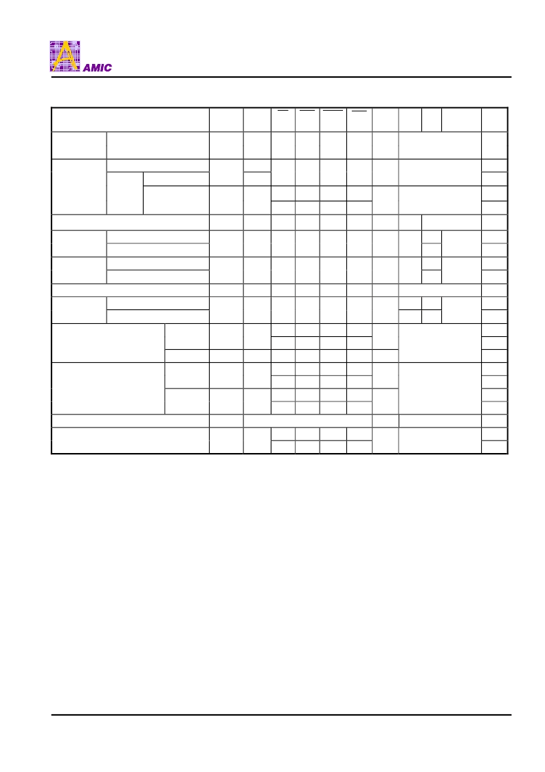
Simplified Truth Table
Command
CKEn-1 CKEn
CS
RAS
CAS
WE
DQM BS0
BS1
A10
/AP
A9~A0,
A11
Notes
Register
Mode Register Set
H
X
L
L
L
L
X
OP CODE
1,2
Auto Refresh
H
L
3
Entry
H
L
L
L
H
X
X
3
L
H
H
H
3
Refresh
Self
Refresh
Exit
L
H
H
L
X
L
X
H
X
H
X
X
3
4
Bank Active & Row Addr.
H
X
X
V
Row Addr.
Auto Precharge Disable
L
H
L
H
4
4,5
4
4,5
6
Read &
Column Addr. Auto Precharge Enable
Auto Precharge Disable
Write &
Column Addr. Auto Precharge Enable
Burst Stop
Bank Selection
Precharge
Both Banks
H
X
L
H
L
H
X
V
Column
Addr.
H
X
L
H
L
L
X
V
Column
Addr.
H
X
L
H
H
L
X
X
V
X
L
H
H
X
L
L
H
L
X
X
L
H
X
L
H
L
H
H
X
X
H
X
V
X
X
H
X
H
X
X
H
X
V
X
H
X
X
H
X
V
X
Entry
H
L
X
Clock Suspend or
Active Power Down
Exit
L
H
X
X
Entry
H
L
X
Precharge Power Down Mode
Exit
L
H
X
X
DQM
H
V
X
L
H
H
X
H
X
No Operation Command
H
X
X
X
(V = Valid, X = Don’t Care, H = Logic High, L = Logic Low)
Note :
1. OP Code: Operand Code
A0~A11, BS0, BS1: Program keys. (@MRS)
2. MRS can be issued only at both banks precharge state.
A new command can be issued after 2 clock cycle of MRS.
3. Auto refresh functions as same as CBR refresh of DRAM.
The automatical precharge without Row precharge command is meant by “Auto”.
Auto/Self refresh can be issued only at both precharge state.
4. BS0, BS1 : Bank select address.
If both BS1 and BS0 are “Low” at read, write, row active and precharge, bank A is selected.
If both BS1 is “Low” and BS0 is “High” at read, write, row active and precharge, bank B is selected.
If both BS1 is “High” and BS0 is “Low” at read, write, row active and precharge, bank C is selected.
If both BS1 and BS0 are “High” at read, write, row active and precharge, bank D is selected.
If A10/AP is “High” at row precharge, BS1 and BS0 is ignored and all banks are selected.
5. During burst read or write with auto precharge, new read write command cannot be issued.
Another bank read write command can be issued at every burst length.
6. DQM sampled at positive going edge of a CLK masks the data-in at the very CLK (Write DQM latency is 0) but
masks the data-out Hi-Z state after 2 CLK cycles. (Read DQM latency is 2)
相關PDF資料 |
PDF描述 |
|---|---|
| A43L2616V-5.5VF | 1M X 16 Bit X 4 Banks Synchronous DRAM |
| A43L2616V-6 | 1M X 16 Bit X 4 Banks Synchronous DRAM |
| A43L2616V-6F | 1M X 16 Bit X 4 Banks Synchronous DRAM |
| A43L2616V-6V | 1M X 16 Bit X 4 Banks Synchronous DRAM |
| A43L2616V-6VF | 1M X 16 Bit X 4 Banks Synchronous DRAM |
相關代理商/技術參數(shù) |
參數(shù)描述 |
|---|---|
| A43L2616V-6 | 制造商:AMICC 制造商全稱:AMIC Technology 功能描述:1M X 16 Bit X 4 Banks Synchronous DRAM |
| A43L2616V-6F | 制造商:AMICC 制造商全稱:AMIC Technology 功能描述:1M X 16 Bit X 4 Banks Synchronous DRAM |
| A43L2616V-6V | 制造商:AMICC 制造商全稱:AMIC Technology 功能描述:1M X 16 Bit X 4 Banks Synchronous DRAM |
| A43L2616V-6VF | 制造商:AMICC 制造商全稱:AMIC Technology 功能描述:1M X 16 Bit X 4 Banks Synchronous DRAM |
| A43L2616V-7 | 制造商:AMICC 制造商全稱:AMIC Technology 功能描述:1M X 16 Bit X 4 Banks Synchronous DRAM |
發(fā)布緊急采購,3分鐘左右您將得到回復。